
Get Your Nitride Quote FAST!
Silicon Nitride Wafer Applications
Silicon nitride (Si3N4) coated silicon wafers are widely used in semiconductor fabrication, MEMS research, and microelectronics. LPCVD silicon nitride films provide chemical resistance, electrical insulation, and protection during various manufacturing processes.
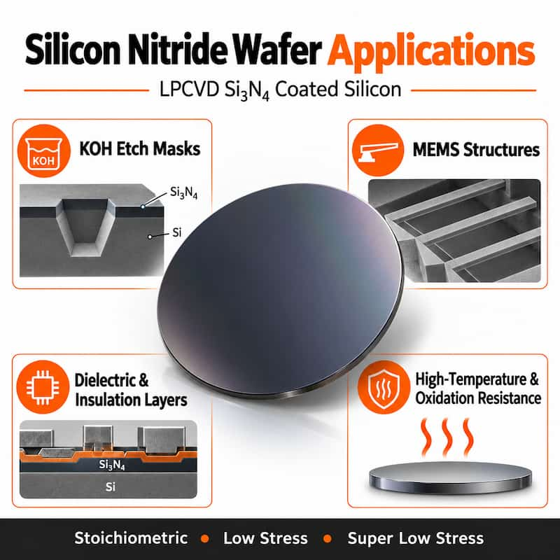
Common Applications of Silicon Nitride Coatings
- KOH Etch Masks: Silicon nitride films act as protective masks during silicon wafer etching, allowing selected regions of silicon to be etched.
- MEMS Structures: Low-stress silicon nitride films are used to fabricate membranes, cantilevers, and other MEMS devices.
- Dielectric and Insulation Layers: Silicon nitride serves as an insulating and protective film in semiconductor devices.
- High-Temperature Processing: Silicon nitride coatings can provide thermal stability and resistance to oxidation in suitable semiconductor processing environments.
UniversityWafer offers stoichiometric, low-stress, and super-low-stress LPCVD silicon nitride coated wafers for research and fabrication. The appropriate film type depends on the required thickness, residual stress, and device application.
We Have the following Silicon Nitride Services
(see below for some inventory)
Stoichiometric LPCVD Nitride
Our Standard nitride film works great as hard mask for KOH etching and can be used as a tool for defining active regions during field oxidation.
Low Stress Nitride
Retains all of the same benefits associated with our standard nitride but can also be used for Membranes, Cantilever Beams and other mechanical structures associated with MEMS devices.
Super Low Stress Nitride
Has been developed for applications that require extremely low film stress. Film Stress can also be customized to meet your unique specifications.
Silicon wafer coatings based on silicon nitride have good high temperature strength, creep resistance and oxidation resistance. Silicon Nitride's low thermal expansion coefficient gives good thermal shock resistance. Silicon Nitride is produced in three main types; Reaction Bonded Silicon Nitride (RBSN), Hot Pressed Silicon Nitride (HPSN) and Sintered Silicon Nitride (SSN). We have Silicon Nitride 2" - 12" all specs and quanities. See silicon wafer diameters for related sizing information.
Silicon Nitride Coating Applications
Silicon nitride (Si3N4) thin films are used as protective and functional layers on silicon substrates. LPCVD nitride can serve as a diffusion barrier, an electrical insulating layer, or a selective etch mask. The appropriate film depends on the device design, process temperature, and mechanical stress requirements.
For MEMS fabrication, low-stress nitride films are often selected for suspended membranes and cantilever structures. Stoichiometric nitride is commonly used as a durable mask during wet chemical processing, including KOH silicon etching.
Choosing the Right Silicon Nitride Film
When selecting a nitride-coated wafer, consider both film thickness and residual stress. Thicker coatings can provide more etch-mask durability, but film stress may also affect wafer bow or delicate suspended structures. Low-stress and super-low-stress options are useful when mechanical deformation must be minimized.
Silicon nitride can also be combined with thermal silicon dioxide in multilayer stacks. Confirm the layer thicknesses, surface requirements, and compatibility with downstream processing before ordering.
Specifications to Include in Your Quote
To help identify a suitable silicon nitride wafer, provide the wafer diameter, orientation, conductivity type, resistivity, substrate thickness, requested nitride thickness, and preferred film type (standard, low stress, or super low stress). If your application requires specific bow, warp, or stress limits, include those requirements in your request.
Fill out the form for an immediate quote.
Below are just some of the silicon wafers coated with silicon nitride that we have in stock!
Below are just some of the Silicon Nitride Coated Wafers that we have in stock! Click Here To Buy!
| ID | Diam | Type | Dopant | Orien | Res (Ohm-cm) | Thick (um) | Polish | Grade | Qty | 1 Unit | 5 Unit | 10 Unit | 25 Unit | Description |
| 1912 | 100mm | P | B | <100> | 0.001-0.005 | 500um | SSP | Prime | 13 | $90.90 | $64.90 | $54.90 | $39.90 | with 100nm of Standard LPCVD Nitride |
| 1913 | 100mm | P | B | <100> | 1-10 | 500um | SSP | Prime | 14 | $69.90 | $64.90 | $54.90 | $39.90 | with 300nm of Standard LPCVD Nitride |
| 1917 | 100mm | P | B | <100> | 1-10 | 500um | SSP | Prime | 10 | $103.90 | $76.90 | $55.90 | with 100nm of Low Stress LPCVD Nitride | |
| 1922 | 100mm | P | B | <100> | 0.001-0.005 | 500um | SSP | Prime | 1 | $120.90 | $88.90 | $64.90 | with 100nm Super Low Stress LPCVD Nitride | |
| 3028 | 100mm | P | B | <100> | 1-10 | 525um | SSP | Prime | 23 | $105.48 | $81.48 | $69.48 | $59.88 | WITH 2 Layers: 500nm Wet Thermal Oxide, and, 40nm Nitride |
Related Silicon Nitride Research & Resources
Explore additional UniversityWafer resources about silicon nitride coatings, semiconductor fabrication, thin films, and silicon wafer research.
- Silicon Nitride Coated Wafers
- Silicon Wafers for Semiconductor Research
- Silicon Substrates for MEMS Applications
- Thermal Oxide Coated Silicon Wafers
- TEOS Silicon Dioxide Thin Films
- Silicon Wafer Diameters and Sizes
- Silicon Epitaxy for Semiconductor Devices
- Silicon-on-Insulator (SOI) Wafers
- Semiconductor Device Manufacturing