What is a Gallium Arsenide (GaAs) MOSFET?
If you are looking for a semiconductor with excellent performance at high frequencies, you should investigate a gallium arsenide metallo-semiconductor (GaAs MOSFET). This material also has outstanding properties in other areas of electronics, such as optical windows, solar cells, and microwave antennas. Listed below are some of the advantages of using GaAs MOSFETs.

Gallium arsenide is a semiconductor material that is used to make a wide variety of electronic devices, including TV and radio transmitters. It also has excellent noise-reduction properties, which make it ideal for use in microelectronics. The high-frequency characteristics of GaAs make it an excellent choice for transparent displays, such as television screens. And with the ability to be miniaturized, GaAs can be used to produce semiconductor devices at higher temperatures.
The benefits of gallium arsenide over silicon include reduced power requirements and thermal noise. While they are more expensive than silicon, they are becoming increasingly popular in electronics, as well as many other fields. In fact, research is continuing to find exceptional uses for this material in a number of fields, including telecommunications and solar cells. However, it is not as fast as silicon, which makes it a better choice for higher-frequency radios.
What Is Gallium Arsenide Used For?
Gallium Arsenide (GaAs) is a semiconductor used in optical scanners in retail stores. GaAs can be made into n-type or a p-type semiconductor by replacing some of the Arsenic (As) with another element.
In addition to its use in electronic devices, gallium arsenide is also an excellent semiconductor material. Its band gap is higher than those of silicon and germanium, while its electron and hole mobility are similar to those of silicon. The chemical formula of gallium arsenide is gallium arsenide (GaAs), with sulfur and selenium used as donor materials. These elements are also substitutes for gallium atoms in other materials.
Gallium arsenide is a semiconductor material made from a combination of Gallium and Arsenic. Its properties are similar to those of silicon, but it is more durable and can be incorporated into more complicated devices. Its electrical and optical properties are enhanced by substituting aluminum for some gallium. The compounds are used in electronics and in many other fields. Nevertheless, research continues to uncover its exceptional uses.
Gallium arsenide is a type III/V semiconductor. It is capable of functioning at high frequencies of 250 GHz, and it does not exhibit thermal noise. Its advantages over silicon include its reduced sensitivity to heat and lower noise level. Its unique properties make it an ideal material for semiconductor devices, and it can also be used for solar cells. Its popularity has led to several developments in the field of technology.
Gallium arsenide is a semiconductor manufactured by replacing part of the gallium with aluminum. It is also a suitable replacement for silicon in linear ICs. As a result, it is a popular choice for a wide variety of applications. Its electronic properties make it an excellent material for a wide variety of electronic devices. But what is gallium arsenide used for?
Gallium arsenide is an important semiconductor made of gallium and arsenic. This compound is a key ingredient in GPS receivers. It has excellent optical and thermal properties, making it an excellent choice for solar cells. Its superiority over silicon made it the ideal material for microchips and lasers. Its properties made it a popular semiconductor. However, it is not a good choice for solar cells.
Gallium arsenide is a semiconductor made from gallium and arsenic. It is also known as III-V compound. Its semiconductor properties are similar to those of silicon and gallium. What is it used for? Its high-purity single crystals are made from this compound. Moreover, its conductive properties make it suitable for solar cell applications. The resulting devices include solar cells and photovoltaics.
The semiconductor gallium arsenide is a type III/V compound that consists of gallium and arsenic. This material is used in many electronic devices. Its unique properties allow it to be a useful semiconductor for various industries. If you are looking for a great solar cell, make sure to check out this material. You will not regret it! So, what is gallium-arsenide?
Aside from being an essential semiconductor, gallium arsenide is also a very valuable metal. Its metal ion conductivity is a very useful quality for a semiconductor. Its metallic shine makes it attractive for laser-guided munitions. Moreover, it is very resistant to abrasion. So, it is not a good choice for microwave-based electronic applications.
This material is an excellent semiconductor. Its high-frequency characteristics make it an ideal semiconductor for radio and TV transmitters. Its metallic shine makes it an ideal semiconductor. It is also used to build optical windows. And it can be miniaturized, which makes it a valuable commodity. Infrared glasses are a great example of glass. They are also made of glass. Combined with a good solar panel, gallium arsenide is a perfect way to save energy.
The chemical formula for gallium arsenide (GaAs) is a III-V semiconductor with a zinc blende crystal structure. Its use in semiconductor technology is very varied. Its use in electroluminescent light-emitting diodes, high-speed magnetic transistors, and monolithic microwave integrated circuits are among its most prominent uses. It is also used in solar cells, low-temperature solders, and as a substrate for other III-V semiconductors.
Why Use Gallium Arsenide?
Compared to silicon, gallium arsenide has lower noise than silicon. Its higher electron mobility makes it ideal for high-frequency devices. This material also offers low-cost semiconductors for high-performance devices. As a result, it is used in many industries, including the electronics industry. And if you're looking for an ideal semiconductor, it can provide a wide range of technological innovations.
This semiconductor material has many uses, and its high-frequency properties make it a good choice for high-frequency devices. Its high-frequency and low-noise characteristics make it an ideal material for optical windows and outer space electronics. These advantages also make it an excellent choice for solar panels. So, you may wonder how gallium arsenide works in such devices. It is one of the few materials that can handle a wide variety of temperatures.
Unlike silicon, gallium arsenide is much more resistant to radiation and heat, making it ideal for fast-switching applications. In addition to these applications, gallium arsenide is an excellent material for LEDs. Its unique properties make it a perfect material for solar cells. So, you should never hesitate to use this compound in your next project. Its versatile properties make it a perfect material for LEDs.
Besides being an excellent semiconductor, gallium arsenide has other advantages as well. It is resistant to radiation and heat, and it is great for high-speed switching. Because of this, it is also an ideal material for LEDs. It can also be used in the construction of laser-guided munitions. Its low-noise characteristics make it an excellent choice for microelectronics.
Aside from being an excellent semiconductor, gallium arsenide is also a versatile material for semiconductors. Its bandgap is higher than that of silicon and allows it to operate at higher frequencies. This means that it can be used in microwave point-to-point links, microwave antennas, and solar cells. It is also used in high-frequency radars and optical windows. Its inherent properties make it a valuable material for a wide variety of electronic applications.
What is a Gallium Arsenide (GaAs) Wafer?
If you are wondering what is gallium arsenide, you have come to the right place. This article will discuss its properties, band gap, and cost. In addition, you will learn about its properties, absorption and emission of light, and band structure. Once you have finished reading this article, you will have a better understanding of what gallium arsenide is. This semiconductor is used for semiconductor applications, including lasers, LEDs, and transistors.
The combination of gallium and arsenic makes gallium arsenide a useful semiconductor material. Its low noise and high-frequency capabilities make it an excellent choice for high-frequency integrated circuits. This material is used in solar cells and microelectronics. Further, it can be used in other applications as well. The semi-insulating properties of the compound make it an excellent material for ultrathin, transparent and infrared-transparent displays.
GaAs is an excellent semiconductor that has both high-frequency and low-noise characteristics. Its unique properties make it ideal for fast-switching devices. It is also a good material for solar cells. Its versatility makes it a popular choice in a variety of industries.
Gallium Arsenide is a semiconductor material that combines the properties of gallium and arsenic. It is similar to silicon but is more durable and can be integrated into more complex devices. Some of the gallium is replaced by aluminum, increasing the material's electrical properties. This material is widely used in electronics and other fields, and research continues to uncover its many unique applications.
The versatility of gallium arsenide wafers makes it an excellent choice for a wide variety of electronic applications. Its low-noise properties allow it to be used in a wide variety of devices. For example, gallium arsenide is a good choice for optical windows, solar cells, and high-frequency radars. It also reduces EPD.
This semiconductor material is used in semiconductor devices, as it is highly resistant to radiation and heat. It is ideal for LEDs and microelectronics. Its low noise properties make it a good choice for transparent displays. There are many more applications for gallium arsenide, and they are more common than ever before. You can find it in consumer goods stores, online and in retail outlets.
What Does Gallium Arsenide Cost?
Gallium arsenide and silicon are two semiconductor materials that start the process of going from raw crystal to electronic device. During the manufacturing process, semiconductor manufacturers form these materials into circular wafers, or discs of purified material. Once these are assembled, subsequent manufacturing steps create the actual electronic device on top of them. Gallium arsenide wafers can cost $5,000 or more, while silicon wafers are only a few dollars.
The technology behind gallium arsenide semiconductors is relatively new, but it has several technical advantages over silicon. Silicon is more affordable by 1,000 times, and it is used in millions of electronic devices, including cellphones. Gallium arsenide chips have the ability to process higher-frequency radio signals more quickly than silicon wafers. Stanford researchers have developed a manufacturing process that can make these devices at affordable prices. They also hope to use these semiconductors in solar panels.
What is Gallium Arsenide Band Gap?
Gallium arsenide is an important semiconductor with a direct band gap. This material is found in the third and fifth columns of the periodic table and is rapidly gaining prime importance in the world of technology. GaAs quantum-wells and bulk semiconductors have been used to build optically active devices. The direct band gap of gallium arsenide is 1.43 eV at room temperature.
The direct band gap of gallium arsenide is 1.12 electron volts, which is much larger than the gap found in silicon. The direct band gap of gallium arsenide semiconductors is determined by extrapolating the square of the absorption curve along the x-axis. This technique is known as the Tauc method. This semiconductor is also called a direct band gap because its minimum conduction band is directly over the maximum of its valance band.
The band structure diagram of gallium arsenide shows the energy of electrons versus their wave number. The subscripts in E are the energy level, whereas the Miller indices represent the Ori of the atomic plane within the crystal lattice. The band gap energy is also close to the energy levels of silicon and germanium. In fact, the energy band gap of gallium arsenide is twice as large as the band gap of silicon. However, the intrinsic carrier concentration of gallium arsenide is far smaller than silicon. In addition, its intrinsic resistivity is eight orders of magnitude larger than silicon.
What is Gallium Arsenide's Absorption and Emission of Light?
This work investigates the optical transport properties of nanowires fabricated from submicrometer GaAs particles. Various fabrication parameters were optimized to achieve maximum scattering and minimum absorption. These samples were characterized with scanning electron microscopy and x-ray diffraction, and the mean-free path was calculated using time-resolved and continuous-wave techniques. Total reflection measurements revealed that these materials show high absorption.
Several advantages of gallium arsenide include its ability to absorb light and emit it. It is also effective at handling high-frequency signals, allowing it to be used in power amplifiers in most mobile phones. Unlike silicon, gallium arsenide exhibits very low circuit noise, making it ideal for use in mobile phone power amplifiers. The material has several applications in space research and is used in a wide range of other devices.
Optical properties of gallium arsenide were investigated to understand the mechanism of the GaAs deep-center laser. This device exhibits optical gain and spectral shift with increasing injection. In addition, the GaAs deep-center laser is capable of tuning from half to bandgap states. The GaAs deep-center laser is a very efficient light source, and its spectral range is approximately 1.54 mm.
What Characteristics Make Gallium Arsenide (GaAs) an Excellent Wafer?
Another important property of gallium arsenide is that it is a type III/V semiconductor. This means that it can function at high frequencies and is relatively noise-free. This characteristic makes gallium arsenide an excellent material for optical windows and monolithic microwave integrated circuits. However, these materials are expensive and are not commonly used in electronics. Therefore, it is crucial to ensure that you understand the benefits and limitations of these materials before starting a project.
Gallium arsenide is a type III/V semiconductor that functions at extremely high frequencies. Because of its high frequency capability, gallium arsenide transistors are also capable of operating at a much higher frequency than silicon. Their high noise resistance makes them a good choice for microwave-frequency integrated circuits, optical windows, and other devices. Lastly, they are highly reflective, making them a great choice for LEDs.
Gallium Arsenide (GaAs) Device Applications
For high-performance integrated circuits, high-performance devices can use gallium arsenide. This compound semiconductor has excellent thermal and physical properties, and is used for light-emitting diodes. It is also used to replace silicon in linear and digital ICs. Linear devices are often used in oscillators and amplifiers. Digital devices are widely used in computer systems, switches, and electronic circuits
Gallium Arsenide Wafers Benefits over Silicon Wafers
One of the main benefits of gallium arsenide over silicon is that it allows electrons to move faster. This makes gallium arsenide an excellent semiconductor material for fast-switching applications. This material is also highly resistant to radiation and heat, making it a great choice for military applications. It is also used in LEDs and displays. But these are just a few of the possible uses of gallium arsenide.
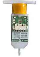
Gallium Arsenide Hall Effect Sensor
A GaAs Hall magnetic sensor used to detect magnetic fields then sends the analog signal for position detection. Below is a BLTOUCH Hall Effect Sensor used to help level the beds of 3D Printers for more preceise prints.
 The Gallium Arsenide Hall Effect Sensor is a semiconductor device that measures the mobility of electrons. Its final output voltage depends on the temperature, and is characterized by a red line cross-shape. At -40 deg C, the highest measured Hall voltage is V H = 72.5 mV. As the temperature increases, the output signal decreases, because increased temperature causes carrier scattering. As the temperature rises, the mobility of carriers of the Hall sensor decreases, resulting in a lower output signal.
A gallium arsenide hall effect sensor can tell the current position of a drive element by reporting a change in the hall voltage. This type of sensor can report both linear and angular positions, and can also work digitally. The drive element typically moves between two end positions, or between the open and closed latch positions. The closed position is set on installation. The other end of the device is the sensor.
The Gallium Arsenide Hall Effect Sensor is made of silicon and Gallium Arsenide. The semiconductors in these sensors are engineered to exploit quantum effects to produce superior performance in real-world metrology. The new sensor is based on silicon and can replace KSY44 and THS119. Its sensitivity is similar to that of silicon. However, the CYSJ902 series can be used to replace a KSY44.
Gallium Arsenide (GaAs) Fast Electronic Switching
The properties of gallium arsenide are highly attractive for fast electronic switching. For one, it can  conduct electricity more efficiently than silicon, which makes it an excellent candidate for fast-switching devices. Other benefits of gallium arsenide include its resistance to heat and radiation, making it a great material for LEDs. Lastly, it can give off light. For this reason, it is a desirable material for LEDs.
Gallium nitride can be a good candidate for LEDs. This material has a wide bandgap, which allows electrons to move faster. This material is highly conductive, which is a major benefit when it comes to fast electronic switching. Additionally, gallium nitride is radiation- and heat resistant, which makes it an ideal material for LEDs. The light emitted by a gallium nitride LED can be seen for miles.
The other major advantage of gallium nitride over silicon is the lower cost of manufacturing. The switching frequencies and energy density are higher with gallium nitride, and the devices are less dense. They also tend to be less dense and are therefore more affordable to manufacture. These factors make it a good option for fast electronic switching. It can be used in mobile phones, radar systems, and higher frequency point-to-point links
Gallium Arsenide (GaAs) Solar Panels
When it comes to solar cell performance, gallium arsenide is the material of choice. Its high efficiency makes it more than twice as efficient as silicon solar cells. This is a significant difference, especially when considering the efficiency of a car battery, which is a critical factor in driving costs. Compared to the former, gallium arsenide solar cells generate about 240 W per square meter under standard test conditions.
 The materials in gallium arsenide are much more effective than those made from silicon and other common materials. These panels also have the best performance of all the types, but their price tag can make them out of reach for many people. That said, as technology continues to improve, it is likely that solar panels will become more affordable for the average homeowner. And even though the prices of solar panels are expected to go down in the future, the material that makes them so effective has a long history of use in semiconductors.
Gallium arsenide solar panels are more efficient than their silicon cousins in a variety of scenarios. In fact, gallium arsenide solar cells can operate at temperatures up to 250 degrees Celsius, which makes them the perfect material for astronauts. These solar panels are also cheaper to produce and can be installed almost anywhere. They are ideal for both residential and commercial use, and are a great investment for your home or business.
GaAs solar panels are more robust for space applications than silicon based solar panels as gallium arsenide modules handle high temperatures better.
high temperatures
GaAs solar panels are insensitive to heat. It is also resistant to radiation.
Gallium Arsenide (GaAs) Light Emitting Diodes
Gallium Arsenide is a semiconductor that emits large amounts of low-brightness infrared radiation.  This light has a short wavelength of 850nm to 940nm. An electrical current flows through the junction, producing light. As the electrical current increases, so does the light output. These diodes are often used as night lights, and the technology has several applications.
However, this material is not particularly flexible. The material's band gap has an effect on the wavelength. For example, a 1.9 electron-volt band gap means that the LED emits more red light than the usual 850nm. A gallium arsenide LED's wavelength can be adjusted by mixing it with another semiconductor, usually gallium phosphide. This can be done by adjusting the ratio of phosphorus to arsenic.
The band gap of an LED affects its wavelength. A gallium arsenide light-emitting diode has a band gap of 1.4 electron-volts. This is the standard for most LEDs, though there are some exceptions. Generally, a GaAs LED produces more visible red light. Nevertheless, if a light-emitting diode's band gap is too low, it will not be effective for certain applications.
In order to extend the lifetime of a light-emitting diode, it is important to add additives. The use of Sn in the substrate has an effect on the brightness of a light-emitting diade. These materials are often cheaper and more efficient than pure GaAs. This is the reason why GaAs is more widely used than other material.
Video: LEDs
What is the Refractive Index of Gallium Arsenide (GaAs)?
Gallium Arsenide (GaAs) is a compound III-V semiconductor that includes both gallium and arsenide. GaAs substrates are used to fabricate the following electronic devices:
- Microwave frequency integrated circuits
- Monolithic microwave integrated circuits
- Infrared light-emitting diodes
- Laser diodes
- Solar cells
- Optical windows
For a typical sample of GaAs the refractive index and extinction coefficient at 632.8 nm are 3.85744 and 0.1983491. Below are files of complete refractive index and extinction coefficients. If the file is not available for download, you can request our proprietary file by clicking "Request".
Gallium Arsenide (GaAs) Wafers for Terahertz-Light Generation
A research client ask if we could help them:
We are looking for GaAs wafers for terahertz-light generation. Could we ask about the cost and availability of the following item?: - undoped GaAs. - polished on both sides. - [110] Ori. - 1" diameter (or 2"). - 0.5 mm thickness. We find that the part number 2313 matches our needs, except for the size (we prefer smaller 1" diameter).
UniversityWafer, Inc. quoted and researcher purchased:
2" Undoped, GaAs, <110> 500+/-20um, 1flat
Notched 150mm Reclaimed Gallium Arsenide Wafers
Research clients have purchased:
150mm Undoped SI Reclaimed GaAs (100) 525um DSP N-type, Epi Ready
We plan to use Bulk GaAs with some test pattern to run some etch process/hardware development trials for a VCSEL & BSV type process.
Researcher asked the following Questions and our reply:
Thank you for the questions, your answers are below:
Q1) Can you confirm that these are notched wafers?
A1) Yes, they are notched.
Q2) Do you only have 25 in stock?
A2) Yes, we stock 25 pcs. We can deliver more if needed.
Q3) Are you likely to replenish your inventory on a regular basis?
A3) Yes, that is correct.
Undoped Gallium Arsenide Wafers
A researcher asked the following: I need an informal offer for some semiconductor Wafer (disc shape). The specifications must be the same for each material: - diameter 2"/3" or something similar -thickness 1 mm or something similar -both faces polished -Undoped The materials of interest for me are: Silicon, Germanium, GaAs, GaP and InP. If there is something available, please let me know the cost.
What Does it Mean Undoped SI GaAs?
(A1) Undoped GaAs means that the GaAs was not intentionally doped during the ingot growth process. There was no dopant added during ingot production. SI means that the material is Semi Insulating which corresponds to very high resistivity ~1.18E8 Ohm-cm.
(Q2) We are talking abut a wafer of crystaline pure GaAs?
(A2) We are talking about the purest GaAs monocrystalline material that money can buy. During the growth process the GaAs is melted in the crucible. The impurities are coming from the quartz crucible to the melt (and from the melt to the crystal). Majority of them are Si atoms. After the ingot production is finished the impurities are present in the bulk crystals. In the result no crystals are 100% pure. However, the amount of impurities is very small.
What Gallium Arsenide Wafers are Used in Monolithic Microwave Integrated Circuits (MMIC)?
Researchers have used undoped GaAs substrates for their MMIC research. The GaAs Integrated Circuits are fabricated to operate at 3 to 300 GHz. To meet this high speed requirement for switching we would suggest using Semi-Insulating GaAs wafers with Ro>1E7 Ohm-cm to prevent high current induction in the circuit. For integrated circuits (rather than individual transistors) it is best to work with (100) Ori {rather than (111) or (110).
Please let us know if you have any questions.
What is a Common Doping Level for Gallium Arsenide Wafers?
A researcher had the following request: For the other specs: 100mm diameter, single-side polished, and high purity. The 1E15cm^(-3) electron concentration is the biggest concern for us, since it looks like it is not a common doping level for GaAs.
UniversityWafer, Inc Answer:
For the quantity, we only need just one 100mm diameter wafer, if possible. If just one is not possible, we may be able to purchase more depending on the cost.
Item Qty. Description
GW75. 1/2/3 Gallium Arsenide wafers, Prime Grade, P/E 4" (100.0±0.1 mm)Ø×625±50µm,
VGF n-type GaAs:Si[100]±0.5°, Ro=(0.038-0.132)Ohmcm,
Nc=(1.6-3.1)E16/cc, u=(1,808-3,229)cm²/Vs, EPD<4700/cm²,
One-side-polished, back-side matte etched, EJ Flats,
Sealed under nitrogen in single wafer cassette.
Undoped GaAs has mobility <4000 and carriers concentration ~1E16. The carriers are naturally coming from the crucible to melt during the growth process. The mobility you mention (~8000) is theoretically possible for GaAs epitaxial layers only, not for bulk materials. GW75 wafer is the one with the characteristics that are state-of-the-art technology and the closest possible to your requirements.
High-Efficiency Photo-Electron Conversion Devices
Researchers have used the followign GaAs Wafers for their experiments. Reference SO30516.
Item #T3882
100mm Undoped GaAs (100) SSP 625 micron SSP
Item #3F120
50.8mm P-type Zinc doped GaAs (100) 350 micron SSP
Item #A1494
76.2mm P/Zn GaAs (100) 400 micron SSP
Why is Gallium Arsenide Used in LEDs?
Gallium arsenide is a semiconductor material used to produce light-emitting diodes. It emits large  amounts of infrared radiation in the 850 to 900 nm wavelengths. During manufacturing, a forward current flows through the junction of the two materials, allowing them to produce light. This type of LED has a high light output, but is not a good option for outdoor lighting.
This substance is so stable that it can be used to produce high-frequency oscillations of electrical currents. This phenomenon is called the Gunn Effect. It is used in the production of LEDs, as well as in other electronic devices. As a result, it is used in the manufacture of lasers and in optical communications. Unlike the fluorescent tubes, LEDs can be made in different colours.
LEDs are made from a semiconductor material such as silicon or gallium arsenide. Neither of these materials is suitable for LED production because they have a wider band gap than silicon or germanium. The latter two are also better suited for manufacturing LEDs, but their price is higher. So, the decision to use gallium isn't entirely based on science.
Despite its disadvantages, gallium arsenide has many technical advantages over its rival, silicon. The former is cheaper to produce, but is more expensive. However, it has higher melting point. Moreover, it has a longer life span compared to the former. As a result, LEDs can be used in various applications. It is also used in military applications. Since it contains a large amount of arsenic, it is regarded as a hazardous material and is therefore a poor choice for many industries.
Why is Gallium Arsenide Better Than Silicon?
When evaluating the two most common semiconductor materials, it's crucial to keep the technology evolving and experimenting with new ones. The most popular material is silicon, and it is incredibly cheap to manufacture. However, there are many other advantages to using gallium arsenide in your designs, and these are worth exploring. This article will outline the main differences between the two, and highlight some of the technical benefits of each material.
Gallium arsenide offers several material-technical advantages over silicon. The fastest transistors are  made from gallium, which is faster than silicon and has a higher electron mobility. In addition, gallium arsenide can handle high-frequency radio signals. Unlike its competitor, gallium is a non-conductor, making it ideal for a variety of applications, including photovoltaics.
Another advantage of gallium arsenide is its greater electron speed, which is five times faster than that of silicon. While silicon is a semi-conductor, gallium arsenide offers a wider operating range and greater radiation hardness. It is also more resistant to heat than silicon, making it an attractive choice for a wide range of applications. In the future, we might even use this material in electronic devices.
While silicon is the most common semiconductor material, the upcoming material gallium arsenide is a superior option. Its electrons move much faster than silicon, and its crystalline structure is more stable than that of silicon. It also allows for a wider range of operating temperatures than silicon, which is why it's ideal for a high-frequency radio signal processor. Aside from being more reliable than the latter, gallium is a much cheaper option than silicon.
The material gallium arsenide is much cheaper than silicon. In fact, it is about 1,000 times more expensive than silicon. The advantage of gallium is that it has lower defect rates than silicon. Additionally, it is much less prone to heat than its rival. Nevertheless, it is not a substitute for silicon in electronics. It has many advantages over both. The most obvious of these are its ability to produce semiconductor devices at higher operating temperatures.
Aside from being cheaper than silicon, gallium arsenide is a better choice for a semiconductor in a wide range of applications. Its higher electron speed is an important factor in determining the best semiconductor for your needs. In addition, it has wider operating temperatures and radiation hardness than silicon. In addition to that, it can be used in solar cells and power plants. Its higher cost makes it a better choice than silicon for most applications.
In contrast to silicon, gallium arsenide is much cheaper. It can be grown on a larger scale and in more convenient shapes, and it is more durable than silicon. Moreover, it's a better choice for high-frequency radio signals. It is also relatively insensitive to heat and is ideal for solar energy. In summary, why is gallium arsenide better than silicone?
The main benefit of gallium arsenide is its faster electron speed, which is five times faster than silicon. Its lower defect rate is also a key factor. Its high temperature resistance is a crucial feature for semiconductors, while its lower radiation hardness makes it a superior choice for mobile phone screens. It is cheaper than silicon but not quite as fast as its rival. The cost of gallium arsenide is comparable to that of its competitor silicon.
In terms of electron mobility, gallium arsenide is far more efficient than silicon in a wide range of applications. A single-crystal GaAs device can function at over 250 GHz, which is very important for power MOSFETs. Despite its cost, it's a better choice for microwave point-to-point links and radar systems. You'll be glad you did.
A direct bandgap allows light to pass through. This makes gallium arsenide a better choice for semiconductors. A direct bandgap is an important feature of solar cells and other semiconductor devices. A semiconductor with a high-energy bandgap is more efficient than one with an indirect one. Further, a direct-bandgap GaAs wafer is better for absorbing higher-energy photons than silicon.
GaAs Wafer Benefits
Watch https://www.youtube.com/embed/uEETZku6ILg
Why is Arsenide Used in Semiconductor Devices?

Why is arsenide used so much? The main reason is that it is cheaper than silicon. Gallium arsenide is a promising material for semiconductor applications and is expected to replace silicon in many types of integrated circuits. It is also faster than silicon at transmitting signals, making it an attractive choice for supercomputers. Fortunately, the Ford Motor Co. is the first company to commercially produce gallium-arsenide chips in large quantities for the open market.
Arsenide is a semiconductor made of gallium and rhodium. It is a type of compound with eight valence electrons and is therefore well-suited for amplifiers and diodes. However, this compound is more difficult to manufacture than silicon, and the chemical process to produce it is toxic. Fortunately, the technology has made gallium arsenide one of the most common materials used in semiconductor devices.
The main difference between gallium arsenide and silicon is that gallium is a metal and gallium has an uncharged valence electron. Gallium is more conductive than silicon, which is why it is more expensive than silicon. The downside to this is that gallium is less common than silicon, which makes it a less cost-effective material for semiconductor applications. It is still used in certain semiconductor applications.
Another reason gallium arsenide is used in semiconductors is its ability to make high-frequency signals. Its relatively low toxicity means that it is ideal for the production of microwave devices, and gallium is less expensive than silicon. But it's not without its drawbacks. Despite its low cost, the chemicals used to make it are highly toxic and can cause cancer. And the Illinois group is currently exploring the possibilities for more innovative applications for this material.
This compound has numerous benefits. Its high-frequency properties make it a great candidate for high-frequency applications. It is an excellent choice for a number of applications. It can be used for a wide range of electronic components. The technology isn't limited to transistors. The use of gallium arsenide in semiconductors includes optical windows and monolithic microwave integrated circuits.
Unlike silicon, gallium arsenide is toxic. It is difficult to manufacture, and requires a lot of energy to make a high-frequency device. It is also cheaper than silicon and gallium nitride, but it is harder to work with. The chemicals used in semiconductors are toxic and are not suitable for human consumption. It is advisable to contact a qualified technician for any questions related to its composition.
As a type III/V semiconductor, gallium arsenide is a great alternative to silicon. Its low-cost properties make it an attractive choice for chip manufacturing, but the main disadvantage is its cost. In addition to being expensive, gallium is also toxic, making it difficult to use in chip manufacturing. In the semiconductor industry, gallium is commonly used as a key component of transistors.
The main advantage of gallium arsenide is its ability to produce silicon, but it is also cheaper. The compound is more toxic than silicon and is a better candidate for use in solar cells and other electronic devices. The University of Illinois is a pioneer in compound semiconductor manufacturing, and the team has been a major contributor to the development of the technology. Its researchers include professor Xiuling Li and postdoctoral researcher Sung-Jin Jo, and postdoctoral fellow John Rogers.
The main advantage of gallium arsenide is its high-speed capability. Its transistor rate is up to five times faster than that of silicon. But silicon remains the most common semiconductor material. It is also used in high-speed VLSI designs, but other materials may still be used as well. If you are looking for a semiconductor, it is important to choose the right one. It is not easy to find a material that can work in many different applications, so it is important to check a few examples.
The main advantages of gallium arsenide are its increased thermal resistance, low power consumption, and reduced power requirements. The U. of I. 's new research shows that the material is more versatile than silicon. Despite its price, gallium arsenide is becoming an increasingly popular semiconductor. It is being used in everything from telecommunications equipment to computer monitors. Its high speed is the basis of its success in the field.
GaAs in Semiconductors
Watch https://www.youtube.com/embed/sfTXZP2DB20
What is the Voltage of Gallium Arsenide Diode
One of the most common questions asked by electronic engineers is "What is the voltage of gallium arsenides?" The answer to this question depends on the diode's physics. In a power gallium-arsenide (GaAs) diode, Vs is the power supply voltage, while VrefA is the reference voltage. The former is the reference voltage for the device, while the latter is the source of the current.
The difference between the two voltages is related to the fabrication process. The temperature changes cause the resistance of a semiconductor, such as gallium-arsenide (GaAs), to change. The voltage drop across the GaAs diode decreases with increasing temperature, while the current Ibs tends to increase as it reaches the node 16. This rise in current causes a reduction in the reference voltage VrefB, which shifts the operating point back to its nominal 3.7-volt operating point.
The variation in voltage across the GaAs diode is due to both temperature and fabrication process. Increasing temperature increases the resistance of the diode, while the temperature decreases the resistance. The current I A has a constant voltage drop across the GaAs diode. The constant current I A provides the constant current required. The resistance Vds of the GaAs FET Q1A operates at its nominal voltage of 3.7 volts.
What Gallium Arsenide Wafer is Used for Harmonic Generation (SHG) Experiments?
Scientists:
I would like to purchase a GaAs wafer for my second harmonic generation (SHG) experiment. I think GaAs[111] has the strongest SHG signal. If yes, would you send me a quote for it?
UniversityWafer, Inc. Quoted:
| Item |
Typ/Dop |
Orient. |
Diam. |
Thck
(μm) |
Surf. |
Resistivity
Ωcm |
Nc
a/cm3 |
Mobil
cm2/Vs |
EPD
/cm2 |
Comment |
| 6272 |
P/Zn |
[111B] ±0.5° |
2" |
300 |
P/E |
0.10-0.12 |
(2.8-3)E17 |
193-208 |
<5.7E4 |
SEMI Flats; Epi Ready |
| 6974 |
N/Te |
[111] ±0.5° |
1" |
500 |
P/P |
0.00245 |
8.21E17 |
3,101 |
<5E4 |
NO Flats; Epi Ready |
| 7932 |
Undoped/SI |
[111A] |
2" |
500 |
P/E |
n-type 1.22E9 |
N/A |
2,154 |
<65,000 |
Diced into 5mm x 10mm rectangles (22 rectangles) |
| 8110 |
N/Si |
[111A] |
2" |
750 |
P/P |
0.0257-0.0678 |
(3.8-8.77)E16 |
2,441-2,766 |
<1E5 |
P Flat @ <11-2>; SF 45° CCW from PF; Epi Ready |
| 8204 |
N/Si |
[111B] |
2" |
350 |
P/E |
N/A
|
(2.27-2.31)E17 |
N/A |
N/A |
2 Flats; Epi Ready |
| A204 |
N/Si |
[111B] |
2" |
350 |
P/E |
0.00171-0.00236 |
(1.13-1.34)E18 |
2,328-2,707 |
N/A |
P Flat @ <11-2>; SF 45° CW from PF; Epi Ready |
Reference #265444 for pricing.
What are Photonic Crystal Surface-Emitting Lasers?
Photonic crystal surface-emitting lasers (PCSELs) are a type of laser that uses a photonic crystal structure to generate and amplify light. Photonic crystals are materials with a periodic arrangement of dielectric materials that can control the flow of light through the material.
In a PCSEL, the photonic crystal structure is used to form a resonant cavity that confines and amplifies the light generated by the laser. The light is then emitted from the surface of the device, rather than from the end of an optical fiber or from a semiconductor gain region as in traditional lasers.
One of the key advantages of PCSELs is that they are able to generate highly directional, high-quality beams of light, which makes them useful for a variety of applications, including telecommunications, sensing, and imaging. PCSELs are also highly efficient, and they are able to operate at low powers and at a wide range of temperatures.
PCSELs are typically made using semiconductor materials, such as gallium arsenide (GaAs) or indium phosphide (InP), and they are often fabricated using advanced microfabrication techniques, such as photolithography and etching.
Why is Gallium Arsenide Used in LEDs?
A common diode material is gallium arsenide. This substance has a band gap of 1.4 electron volts and emits infrared at a wavelength of 900 nanometers. Learn more about GaAs and GaN and how they work. Then, you can decide which one will work best for your LED. In this article, I'll explain the differences between GaAs and GaN and show you how to tell them apart.
How Important Are GaAs Wafers in LED Production?
Gallium arsenide is an important ingredient in the production of LEDs. It is used in optical communications, control systems, and other electronic devices. It is also used in the manufacture of integrated circuits (ICs), where it can replace silicon. Linear devices use the material for electronic switching and oscillators, while digital devices are used in computer systems. These electronic devices are called systems of systems.
In a conventional LED, the n-type has extra electrons, while the p-type has too many holes. When the current passes through the p-n junction, the electrons and holes swap sides. The current then recombines them into light. Modern LEDs can emit a wide range of colors, including infrared light, which has an infrared wavelength of 760 nm and a voltage of 1.63 volts.
GaInN LEDs are an example of this new material. These diodes use a combination of three LEDs tuned for the appropriate output levels. They are also made up of a semiconductor called indium nitride. A blue LED can produce white light by adding a white LED. A white LED may also be made of three or four diodes, depending on their sensitivity.
Because of the bad gap, GaN is able to shed a large amount of energy in the form of visible light. LED lights produce a full spectrum of colours, which makes them very useful for a wide variety of applications. They also use less electricity than halogen lights and backlight liquid crystal displays. GaN is stable at higher temperatures than other semiconductors and therefore does not require perfect crystals. The compound is formed by heating Ga(CH3)3 and ammonia.
AlGaAs red LEDs are the first LEDs to surpass the luminous efficiency of filtered incandescent lights. They soon replaced the light bulbs in many exterior lighting applications, including center high mount stop lights on motor vehicles. AlGaAs red LEDs are produced by crystal-growth techniques, and they have an advantage over other red LEDs. A red LED can also emit a high degree of visible red light compared to a green one.
A transparent substrate chip is one of the most important design features of LEDs. This type of chip can extract more light from its side surfaces, which increases the efficiency of the LED. Often, hybrid designs are created, which incorporate a substrate with intermediate properties. Another important factor is the graded change in refractive index. Phosphors can be enhanced to improve light extraction efficiency, but the biggest hurdle to a high level of efficiency is the Stokes energy loss.
A semiconductor material such as GaAs produces large amounts of low-bright infrared radiation. The wavelengths of the light are in the range of 850nm to 940nm. A junction made of GaAs is a convenient place to produce these materials. When combined with silicon, they create high-power LEDs. They are also useful in space electronics. A recent study revealed that GaAs is used in solar cells.
The mixed-crystal ratio of this material is selected depending on the emission wavelength desired. It can be either green or blue. The blue/green LEDs were made available in the late 1990s and have been increasingly popular in commercial applications. But AlGaN has not reached the efficiency of blue/green LEDs. This material emits light in the near-ultraviolet range with wavelengths of 350-370 nm.
Why is gallium arsenide used? It was discovered in 1875 by Paul-Emile Lecoq de Boisbaudran. His initial experiments using a crystal of silicon carbide and a cat's-whisker detector produced the first commercial red LEDs. His work was later published in Russian and German journals and did not become practical for consumer electronics until decades later. In 1955, Rubin Braunstein first reported that GaAs and gallium arsenide emit light in the infrared range.
LED is a semiconductor chip. It has a lead frame connected to two electrical wires. The semiconductor chip has two distinct regions - p and n. The electrons are injected into the p region and combine with a hole to release energy in the form of a photon. This energy is converted into light. And this process is called LED. So, why is gallium arsenide used in LED?
Gallium Nitride (GaN) LEDs
Gallium arsenide is a semiconductor compound used in the production of LEDs. Gallium arsenide has a 1.9-electron-volt band gap, while gallium phosphide has a 2.3-electron-volt band gap. Gallium arsenide and gallium phosphide can be combined to produce LEDs with a band gap between 1.4 and 2.3 electron-volts.
The semiconductor compound gallium arsenide emits large amounts of low-brightness infrared light in the wavelength range 850nm to 940nm. It produces light when electrons lose energy in small packets. Since the semiconductor is transparent and insulating, the energy produced by electrons in the LED is stored in the light-emitting material. Therefore, the wavelength of light produced by the LED is longer than that of conventional light sources.
Gallium is a metal with little structural value. In fact, its main usage in modern electronics is as a semiconductor. GaAs wafers account for about 70% of the annual consumption of gallium. High-brightness LEDs are used in mobile screens, for example. Government support for LED lighting has increased as more people realize the energy efficiency of LEDs. So, what are the benefits of using gallium in LEDs?
The GaAs semiconductor can be grown in different ways. First, epitaxial layers of AlGaAs can be grown sequentially on a GaAs substrate. Layers 133 and 135 are p-type Aly Ga1-y As materials, while layers 134 and 136 are n-type Alx Ga1-y As materials. These are referred to as the active layer and the cladding layers, respectively.
A further way to increase LED efficiency is to use Zn diffusion. By using a Zn diffusion process, epitaxial layers are defined. In FIG. 3, an n-GaAs substrate 207 has a n-Aly Ga1-y cladding layer 206. Next, a p-Aly Ga1-x As active layer 205 is formed over the n-Aly Ga1-y cladding layer 207. Then, an n+-GaAs epitaxial layer 15 is deposited on top of the n-GaAs substrate 207. This layer is patterned with a SiN diffusion barrier 202.
Another material commonly used in LED technology is gallium arsenide. Its band gap is 1.4 electron-volts. As a result, it emits infrared light with a wavelength of 900 nanometers. Unlike silicon, the wavelength of light produced by a gallium-aluminum-arsenide device is very short. This means that LEDs are useful for LED applications.
The material also exhibits wide band-gap properties. A blue LED can be made with an addition of Gallium Nitride (GaN). This material has similar color characteristics to fluorescent lamp tubes. GaInN LEDs use blue emission to excite phosphors. This technology can be fabricated into two kinds: pale white and cool white, but bluish in color. The former produces a brighter light, whereas the latter produces a bluish hue.
The main goals of LED construction are to maximize light generation in the chip material and to extract as much of it as possible. A forward-biased p-n junction injects electrons and holes from the p region into the n region. The minority-carrier injection alters the equilibrium charge carrier distribution. Minority carriers then recombine with the majority carrier and the LED returns to thermal equilibrium.
What is a Gallium Arsenide (GaAs) MOSFET?
If you are looking for a semiconductor with excellent performance at high frequencies, you should investigate a gallium arsenide metallo-semiconductor (GaAs MOSFET). This material also has outstanding properties in other areas of electronics, such as optical windows, solar cells, and microwave antennas. Listed below are some of the advantages of using GaAs MOSFETs.
Gallium arsenide is a semiconductor material that is used to make a wide variety of electronic devices, including TV and radio transmitters. It also has excellent noise-reduction properties, which make it ideal for use in microelectronics. The high-frequency characteristics of GaAs make it an excellent choice for transparent displays, such as television screens. And with the ability to be miniaturized, GaAs can be used to produce semiconductor devices at higher temperatures.
The benefits of gallium arsenide over silicon include reduced power requirements and thermal noise. While they are more expensive than silicon, they are becoming increasingly popular in electronics, as well as many other fields. In fact, research is continuing to find exceptional uses for this material in a number of fields, including telecommunications and solar cells. However, it is not as fast as silicon, which makes it a better choice for higher-frequency radios.

 achieved then as thin as thin as possible. Diameter 1 inch - 1.15 inch. We would prefer if the wafers are support free—not on a metal support. I’m not sure if you have to polish the wafers on both sides to achieve the thickness but it is not it is not necessary for us to have the wafers polished. If it is easier for you not to polish then don’t worry about it.
 provides a real advantage over silicon for some components.
 How to Make Laser Diodes with Gallium Arsenide is the subject of an interesting new book. It is a very straightforward process that uses a single semiconductor material - gallium arcsenide. Using the compound, you can make the laser diodes that light up. The key is in making the materials work together in a way that allows them to be both effective and efficient.