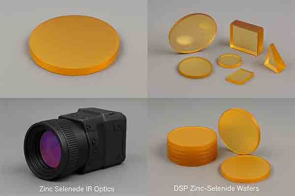
I'm looking for double side polished zinc selenide wafers with low roughness. Do you have some available?
I am flexible on the wafer size. If it is possible to be precut into 15mm x 15mm squares that would also be ideal.
ZnSe Wafers & Substrates
A PhD candidate requested a quote for the following.
UniversityWafer, Inc. Quoted:
| Material | Orientation | Dimensions | Finish |
| ZnSe poly-crystal | Poly-crystal | 101.6mm dia x1.8mm | Fine ground |
| ZnSe poly-crystal | Poly-crystal | 101.6mm dia x1.65mm | Two sides polished, s/d: 60/40-1 |
| ZnSe | 110 | 10x10x1.0mm | 2sp, s/d: 60/40 both sides, High resistivity |
| ZnSe | 100 | 10x5x1.0mm | 1sp - ZnSea100510S1US |
| ZnSe | 100 | 10x5x0.5mm | 1sp - ZnSea100505S1US |
| ZnSe | 100 | 5x5x0.5mm | 1sp - ZnSea050505S1US |
Reference #323557 for pricing.
Get Your Quote FAST! Or, Buy Online and Start Researching Today!
Thick Zinc Selenide Wafers
An ajunct professor requested a quote for the following.
We are looking for ZnSe 1mm thick wafer. (dealy we would like the part to be precision cut to size at 44x50mm, otherwise a disk might do for now. We would need around 5 piece to begin with, depending on the price!
UniversityWafer, Inc. Quoted:
- Size:44x50mm Thickness: 1mm SSP
- Size:44x50mm Thickness: 1mm DSP
Reference #323813 for specs and pricing.
Zinc Selenide Wafers for Material Characterizing
A graduate student requested a quote for the following.
We would be interested in 2", 4" and 6" wafers (5 units of each), with a thickness between 0.5 and 1mm if possible. We have no spec requirements apart from them being pure ZnSe without any type of coatings, since we are interested in characterizing the material.
Reference #325672 for specs and pricing.
Zinc Selenide Reference Temperature
A scientist requested an answer for the following.
Question:
In your description of ZnSe wafers, you mention a high temperature pre-treatment for adhesion promotion. Can you provide a reference temperature or publication that informs the temperature range of the pre-treatment?
Answer:
Short answer: one well-documented “high-temperature pre-treatment for adhesion” on ZnSe is around 300 °C.
Key points from that work:
-
ZnSe windows (1″ dia., 1 mm thick) were annealed on a hotplate at 300 °C for 5–30 min prior to coating.Society of Vacuum Coaters
-
The goal was explicitly to create a better surface for oxide coatings by removing polishing residues and modifying the near-surface composition.
-
After this 300 °C pre-bake, the oxide stacks passed humidity and tape-peel adhesion tests according to MIL-F-48616, whereas untreated samples failed.Society of Vacuum Coaters+1
So if a wafer or optics vendor says “high temperature pre-treatment for adhesion promotion” on ZnSe, a 300 °C pre-bake is a very plausible reference point, and Coşar et al. is the clearest published justification I know of.
For broader context:
-
Multiple ZnSe thin-film and substrate studies use post-deposition or substrate anneals in the 250–350 °C range to improve film structure and interfaces without damaging ZnSe, which is consistent with using ~300 °C as a safe, effective “high-T” surface-conditioning regime.SpringerLink+1
-
Safety data sheets indicate ZnSe starts to decompose or evolve toxic fumes in air only above roughly 400–500 °C, so 300 °C stays comfortably below that.
Reference #315891 for specs and pricing.
Double Side Polished ZnSe Wafers
A postdoc requested a quote for the following.
We need to order Zinc Selenide substrates. I saw on your website that you only have single-side-polished ones. Do you, by chance, have also double-size polished ones?
We don't have very strict spec:
- We are planning to use the ZnSe substrates are substrates for samples for transmission experiments, thus we need DSP and generally high transparency in mid-IR (specifically in the 8-12 um region).
- Thickness can be anything >= 500 um
- We would prefer already-diced substrates with dimensions 2cm x 2cm, if possible. If that's not possible, we can also work with 1cm x 1cm
- Initially we would not order many, maybe 10 - depending on price. If the first experiments are successful we will order more.
UniversityWafer, Inc. Quoted:
We can supply the following: ZnSe substrates with the following specifications:
- 10х10х1 mm, 2 sides polished 60/40 (Scr/Dig)
- 20х20х1 mm, 2 sides polished 60/40 (Scr/Dig)
Reference #270834 for specs and pricing.
ZnSe Wafers For Testing X-Ray Electron Spectroscopy
A PhD candidate requested a quote for the following.
I request the quotation for Zinc Selenide wafer (ZnSe) with dimension of 10*10*0.5 mm or smaller; any surface finish; any orientation; any conductivity type. I will use it to test and obtain x-ray electron spectroscopy for the coating polymer on ZnSe. It would be nice if you could send me the quotations for the ZnSe wafer.
Also, please let me know how long it will take to deliver the product.
Reference #106750 for specs and pricing.
ZnSe For Infrared Experiment
An assistant professor requested a quote for the following.
I would like to receive some informations about Infrared Materials available on your site, Cadmium Telluride and Zinc Selenide in particular.
I would like to know if you can produce and deliver these materials with a
specific thickness, in particular:
0.92’’ and 1.05’’ thickness of CdTe 2.06’’ and 2.29’’ thickness of ZnSe.
I work at Department of Physics, and we
need these materials for some experiments about Infrared techniques, with no
productive purpose.
If not possible, could you suggest me another company which may be available?
Reference #134400 for specs and pricing.
Zinc Selenide (ZnSe) Applications
Zinc Selenide (ZnSe) is one of the most widely used materials in mid-infrared (mid-IR) optics because of its high transmission from 0.5–15 µm, low absorption at 10.6 µm, and excellent mechanical stability. Below are the most important research and industrial applications.

1. CO₂ Laser Optics (10.6 µm)
ZnSe is the industry standard material for high-power CO₂ laser systems, where it is used for:
- Laser windows
- Beam expanders
- Focusing lenses
- Protective optics for industrial cutting and welding
2. Mid-IR Imaging & Thermal Cameras
Because of its wide transmission band and low absorption, ZnSe is used for:
- Thermal camera windows
- Infrared imaging systems (3–12 µm)
- IR spectroscopy cells
- Environmental gas-sensing instruments
3. Waveguides, Filters & Beam Splitters
ZnSe substrates are commonly used for fabricating mid-IR photonics components such as:
- Planar waveguides
- Etalon filters
- Beam splitters
- Acousto-optical modulators
4. Epitaxy & Thin-Film Research
ZnSe films can be deposited by MBE, MOCVD, PLD, and sputtering, and are used to study II-VI semiconductors for optoelectronics. Applications include:
- Blue/UV emitters and detectors
- Heterostructure interfaces with ZnS, CdSe, and GaAs
- Quantum well and quantum dot studies
5. Protective Optical Coatings
ZnSe substrates often require high-temperature pre-treatment (~300 °C) to improve adhesion for:
6. Custom Substrates for Research Labs
- DSP or SSP wafers
- Diced substrates (5×5 mm, 10×10 mm, 20×20 mm, etc.)
- Thickness from 0.5–2.0 mm
- Low-roughness surfaces for transmission experiments
