FD Silicon-on-Insulator (SOI) for Research & Production
What is FD SOI Benefits?
The main problem with making semiconductors is that they use a lot of power and this can lead to overheating.
Solution: FD-SOI is a new technology that solves the power consumption and overheating problems. It has been used to make computer memory and power management chips, and it has several advantages over other technologies, including a high performance capability.
See below for inventory.
Get Your SOI Quote FAST! Or, Buy Online and Start Researching Today!
SOI Wafer Inventory
SOI Item #G4P-017-01 - 100mm P/B (100) 500um14-22 ohm-cm Device 340nm, Oxide 1000nm UNIBOND Prime Grade
(50 wafers left)
(75 wafers left)
SOI Item #G4M-005-01- 100mm P/ B(100) 500um 14-22 ohm-cm Device 340nm, Oxide 400nm UNIBOND Monitor Grade
SOI Wafer Special
SOI - Can't buy many wafers? We can quote you just one wafer.
For example
150mm SOI P/B (100) 625um 1,000 ohm-cm
Device 200nm
Oxide 1,000nm
Don't buy ten if you don't have to!
November Special
- 8" SOI with device layer 50nm thick
-Top Si: p-type/<100>/8.5-11.5 ohm.cm
-Box:0.2um thick
-Handle Si wafer:p-type/<100>/725um thick/15 ohm.cm
The price is
-$590.00/ea for 5 wafers.
-$690.00 each for one
While the supply lasts!
What Are the Advantages of FD SOI?
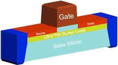
FD-SOI, also known as ultra-thin silicon-on-insulator, is a semiconductor material that is thin enough to be used in electronics. It is a planar process that allows for deep submicron devices. The process starts with a thin layer of epitaxial silicon and is followed by an oxide layer that functions as an insulator. The semiconductor's structure does not contain any intrinsic charge carriers, which makes FD-SOI an excellent choice for deep-submicron applications.
FD-SOI has several advantages over bulk silicon. The technique can reduce device variability by using undoped channels. For example, compared to bulk CMOS, an FD-SOI device delivers higher performance per unit area. Its thinner channel also improves mismatch characteristics. Moreover, the FD-SOI process can reduce the size of a transistor's gate.
FD-SOI is a more advanced process than bulk silicon. It can be produced at 28 nm, which is more advanced than its predecessors. Its lower gate capacitance and higher transconductance efficiency make it a better alternative for low-power applications. This technology is also more cost-effective than bulk silicon. It can reduce device size by up to 40%.
FD-SOI is a better option for low-power applications. The process uses thin undoped channels to decrease device variability. This process has improved the mismatch characteristics of FD-SOI devices. Further, FD-SOI reduces the area of a semiconductor device. In addition, a FD-SOI is more area efficient than bulk silicon. There are a number of advantages of FD-SOI.
FD-SOI is an alternative to bulk silicon, making it easier to process and produce semiconductors. Its thin undoped channels and FD-SOI technology are more reliable than bulk silicon and are thus superior. This process is also a better alternative for deep-submicron devices. Its FD-SOI technology provides better transition efficiency and lower gate capacitance.
FD-SOI has many benefits, and it can be used to produce a variety of types of semiconductors. It has a planar structure that enables it to be manufactured in large quantities. FD-SOI can be made from a slender SiON/TiN layer and an insulator layer. It has the advantage of a shallow-submicron device that can be made into a larger size.
FD-SOI is an alternative to bulk silicon for many applications. It has an epitaxial layer of epitaxial silicon and an insulating layer. It is a good alternative to bulk because it does not have intrinsic charge carriers. Therefore, it is a better choice for deep-submicron devices. However, FD-SOI is less expensive than bulk silicon, but it is still a superior option.
FD-SOI technology is a viable alternative to bulk silicon for many applications. FD-SOI is a layered SOI substrate that is depleted with a buried oxide layer. It offers significant advantages to both FD-SOI and bulk-silicon semiconductors. The FD-SOI technology is also known as a fully-depleted silicon-on-insulator.
FD-SOI is a seminal process that is gaining popularity in the semiconductor industry. Although it has yet to become a common choice, it is still a great choice for manufacturers of portable devices, and even mobile equipment. The FD-SOI process is a highly flexible and cost-effective solution for many applications. It also allows for the use of oxide layers on bulk silicon.
FD-SOI is an alternative to bulk-CMOS technology. Its advantages include lower cost and increased effective electron mobility of transistors. FD-SOI is also better for a wide range of low-power applications. The technology has a very high level of integration, and the advantages of FD-SOI are not only in mobile devices. So FD-SOI is a great choice for many applications.
Below are just some Soitec Silicon-on-Insulator Wafers that we have in stock
| Item | Dia | Typ/Dop | Ori | Res ohm-cm | Handle | Device nm | Oxide μm (or nm) |
| 2327 | 25mm sq | P/B | (100) | 14-22 | 625 | 500 | 3 |
| 2377 | 150mm | P/B | (100) | 14-22 | 675 | 100 | 200nm |
| 2415 | 150mm | P/B | (100) | 13.5-22.5 | 625 | 500 | 3 |
| 2265 | 200mm | P/B | (100) | 9-16 | 725 | 145 | 135 |
| 2266 | 200mm | P/B | (100) | 9-16 | 725 | 190 | 150 |
| 2551 | 200mm | P/B | (100) | 1-20 | 725 | 70 | 2,000nm |
| 2268 | 300mm | P/B | (100) | 9-16 | 775 | 50 | 145 |