As-Cut Silicon Wafers All Diameters for Research & Production
Why Use As-Cut Silicon Wafers?
Manufacturers need a convenient way to produce components, and the as-cut silicon wafer manufacturing process can be difficult and time consuming.
As-cut Silicon Wafers are a convenient way to manufacture components. UniversityWafer, Inc. has as-cut silicon wafer inventory available in most diameters and specs
Get Your As-Cut Si Wafers Quote FAST!
Below are some of the As-Cut Silicon Wafers that we have available.
| Item | Dia(mm) | Typ/Dop | Ori | Thck(μm) | Pol | Res Ωcm | Specs |
| K667 | 6" | P/B | [100] | 900 | C/C | FZ >1,000 | SEMI Prime, 1Flat (57.5mm), |
| E239 | 6" | n-type Si:P | [100] | 825 | C/C | FZ 7,000-8,000 {7,025-7,856} | SEMI, 1Flat, Lifetime=7,562μs, in Open |
| F700 | 6" | n-type Si:P | [100-6° towards[111]] ±0.5° | 790 ±10 | C/C | FZ >3,500 | SEMI, 1Flat, |
| G343 | 6" | n-type Si:P | [112-5° towards[11-1]] ±0.5° | 1,000 ±10 | C/C | FZ >3,000 | SEMI, 1 JEIDA Flat (47.5mm),, TTV<4μm, Lifetime>1,000μs |
| G458 | 6" | P/B | [110] ±0.5° | 390 ±10 | C/C | >10 | 2Flats, |
| F859 | 6" | n-type Si:P | [100-25° towards[110]] ±1° | 800 | C/C | 1-100 | SEMI notch Prime, |
| J724 | 4" | n-type Si:P | [100] | 425 | C/C | FZ >5,000 | 2Flats (p-type flats on n-type wafers), |
| D279 | 4" | Intrinsic Si:- | [100] | 640 ±10 | C/C | FZ >20,000 | SEMI Test, 1Flat,, As-Cut, Edge-Rounded, EDGE CHIPS, cannot be polished |
| E775 | 4" | Intrinsic Si:- | [100] | 615 ±10 | C/C | FZ >10,000 | SEMI Prime, 1Flat, |
| F263 | 4" | P/B | [100] | 480 | C/C | 1--30 | SEMI Test, 2Flats,, UNPOLISHED WAFERS WITH EDGE CHIPS |
| 5420 | 4" | P/B | [100] | 800 | C/C | 0.001-0.005 | SEMI, 2Flats,, With striation marks |
| B752 | 4" | n-type Si:P | [100] | 450 | C/C | 3--5 | SEMI Prime, 2Flats, |
| F975 | 4" | n-type Si:Sb | [211] ±0.5° | 1,600 | C/C | 0.01-0.02 | SEMI Test, 1Flat,, Wafers can be polished for additional fee |
| 5784 | 4" | Si | [110] ±0.5° | 525 | C/C | ? | Empak cst |
| T206 | 3" | P/B | [100] | 3,050 ±50 | C/C | >0.5 | 1Flat, Individual cst (can be ordered singly) |
| TS132 | 3" | n-type Si:P | [111] ±0.5° | 525 | C/C | 0.5-50.0 {0.89-0.98} | SEMI, 1Flat, |
| U206 | 2" | P/B | [100] | 3,150 | C/C | >0.5 | 1Flat |
| 7027 | 2" | p-type Si:Ga | Poly. | C/C | 0.024-0.036 | Gallium doped Concentrate (each with measured Gallium content) | |
| 7LA | 2" | P/B | [100-2.5° towards[110]] | 500 | C/C | 1--20 | Prime, |
| 4427 | 1" | Intrinsic Si:- | [111] ±2° | 27,870 | C/C | FZ >10,000 | Single Crystal Silicon Rod, 0.39" diameter × 27.87±0.1mm |
| 6446 | 0.5" | Intrinsic Si:- | [100] | 12,700 | C/C | FZ >10,000 | NO Flats, a set of 4 rods sealed in polyehtylene foil |
What Are As Cut Silicon Wafers?
As Cut Silicon Wafers are silicon wafers that are not doped on either side. They are also not rounded on the edge. They are packed in coinrolls of 10 wafers and separated with tissues. Polyethylene film is then used to cover the wafers. Then they are packaged in protective packages and shipped to customers. What are As Cuts? Here are some of the advantages.
First, an ingot of silicon is cut into blocks. The first surface is etched, and the etching solution is removed. The  second surface is etched again, making an as-cut silicon wafer with a lower profile. Afterward, both surfaces are polished. After these steps, the wafers are ready to be soldered together. As Cut Silicon Wafers are used for a variety of applications, including semiconductor fabrication, laser sintering, and a wide range of other industries.
As-Cut Si is an easier way to manufacture components. The process involves etching the first surface of an as-cut silicon wafer, removing the etching solution, and then lapping the second surface to create a lower-profile as-cut Si wafer. Once both surfaces are etched, the as-Cut silicon is ready for a subsequent machining process. The as-Cut Wafer is about 180 um thick and has a low-profile.
The manufacturing process for As Cut Si wafers involves two steps. First, a thin layer of organic compounds on the first surface of the wafer is etched. Then the as-cut silicon wafer is cut by a saw. The second etching process is repeated on the second surface, resulting in an as-cut Si wafer with a lower-profile. Once all three surfaces have been etched, the final step is to remove the etching solutions.
As-Cut silicon wafers are a more convenient method of manufacturing components. The first surface of an as-cut Si wafer is etched, and the second is etched, which results in a lower-profile as-cut Si wafer. After etching, the silicon is pre-cleaned and the process starts all over again. This makes the as-cut silicon wafers low-profile.
The As-Cut process is a two-step process. The first stage is the cleaning of the as-cut silicon wafer. Acidic etchants are effective in removing organic and metallic contaminants from the silicon wafer. The second step involves the introduction of a high-dielectric acid and the removal of the carrier membrane. During the first step, the silicon wafer is cut in a ring-like pattern.
The second step is the dicing process. As-cut wafers are the easiest way to make electronic components. In-line etchants can be customized to suit specific semiconductor needs. A low-tack adhesive is applied to the cutting mat. The silicon is then cut. During this process, the silicon is cut into a high-quality as-cut silicon wafer. If the first step is successful, the as-cut silicon wafer is ready for further processing.
As-Cut silicon wafers are an efficient way to produce components. The first step involves etching the first surface, followed by the second step of lapping. The second step involves a second etching process, which removes any residual etching solutions. After the first step, the as-cut Si wafer is ready for the next step in the manufacturing process. It can be a more expensive process, but it will be the best value for your money.
As-cut silicon wafers are the best quality as-cut silicon products. They are more efficient than their traditional counterparts and can be used in a variety of different applications. One of the advantages of as-cut silicon wafers is their high quality and ease of processing. When you use these components, you will be able to produce parts that are compatible with each other. They are easy to manufacture and require no additional tools.
Unlike As-Cut Wafers, As Cuts Silicon Wafers are produced by using a process called dicing. During the dicing process, a silicon wafer is cut using a die that contains a pattern of gold or chromium. As-Cuts are perfect for many applications, but they are also difficult to process. You need a machine with high precision for your application.
What ar As Cut Silicon Wafer Applications?
As-Cut Silicon Wafers are a convenient way to manufacture components. The manufacturing process includes etching the first surface for a first time, and then removing the etching solution. Then, the second surface is etched for a second time to produce a lower-profile, as-cut silicon wafer. The first and second etchant solutions are removed from both surfaces of the as-cut Si wafer.
For high-quality as-cut silicon wafers, acidic etchants are used. The acidic etchant removes 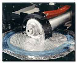 organic and metallic contaminants from the as-cut silicon wafer. The acidic etchant provides a noncontact cleaning method, which supports high throughput. It also allows for fine-tuning the surface roughness of the as-cut silicon. The roughness of the as-cut silicon wafer affects the application of a passivation layer.
An acidic etchant solution is used to remove the oxidizing agent from the as-cut silicon wafer. The acid may contain nitric acid or acetic acids. The as-cut Si wafer may need a filter to prevent silicon carbide enrichment. The as-cut silicon wafer may be pre-cleaned. The organic residues are not removed from this type of as-cut silicon wafer.
Acidic asymmetrical etching is required for As Cut Silicon Wafers. It requires the introduction of a high-dielectric acid to etch the wafers in two steps. The first step involves removing the as-cut silicon wafer from the carrier membrane. The second step consists of fracturing the carrier membrane. This involves introducing a high dielectric density to the carrier membrane.
In-line etching is a process for removing metal and organic materials from as-cut silicon wafers. It is an exemplary process and can be adapted to meet the specific needs of semiconductor makers. The grooved transport rollers are partially submerged in an acidic etchant solution. The etchant solution is diluted with water and the silicon wafer is etched with the same chemical.
The first step of etching is to clean the silicon wafer. In-line etching involves the removal of small amounts of metals and other contaminants from the silicon. The process is continuous and is suitable for high throughput. The second step is to polish the silicon wafer to remove any defects. After the as-cut procedure, the silicon wafers must be cleaned to remove all impurities and contaminants.
The surface of an as-cut silicon wafer contains metallic and organic contaminants. In this case, a pre-cleaning is required. The acidic etchant is a very effective way to remove the metal and organic contaminants from the silicon surface. However, the acidic etchant is not enough to remove all the contaminants. The surface of an as-cut silicon wafe still contains micro-cracks.
Various types of acidic etchant agents are used for cutting Si wafers. These solvents are effective for removing organic and metallic contaminants from silicon wafers. In addition, they are effective at reducing cell degradation. The acidic etchant agents also help control the surface roughness of the silicon. Once the process is completed, the wafers are ready for application of the passivation layer.
While the acidic etchant can be very effective at removing organic contaminants from silicon wafers, it will not be sufficient to remove all traces of these contaminants. The acidic etchant is not sufficient to remove organic and metallic contaminants. Moreover, the process is not compatible with all types of as-cut Si wafers. In the same way, it does not clean the as-cut silicon wafers.
The as-cut process of a silicon wafer has two main advantages. It allows a high-throughput production. One of these benefits is its non-contact nature. Another advantage is the high-waviness process. It is possible to use saw-damaged as-cut wafers for a wide range of applications. Its non-contact etching method is suitable for large-scale as-cut wafers.
After being fully grown, the silicon ingot is cut into blocks according to the desired diameter. The resulting wafers are 180 um thick. The process of cutting a silicon ingot involves several steps. The first is the cutting of the ingot into blocks. This step results in a flat slab of silicon. The second is the lapping process, which cleans the surface of the wafer to remove the saw marks.
What are As-Cut Silicon Substrates
As-Cut Si are wafers that are not polished. The are several steps to making a silicon wafer.
- As-Cut - the unpolished wafers after the ingot is sliced.
- Silicon Lapping
- Silicon Etching
- Silicon Polishing
As-cut wafers are much lower priced than wafers that are lapped, etched and polished. As-cut surface is extremely rough, non-reflective. Our researchers use the as-cut wafers when their research doesn't require polshed wafers. Research includes but is not limited to Solar.
Ask how our as-cut wafers can help you!