Custom Silicon Wafers for Research & Development
Custom Silicon Wafers - Research discounts available!
UniversityWafer, Inc. distributes quality silicon wafers of all grades for semiconductor research and production. Diameters range from less than 1 inch to 12 inch. Our custom wafer service means we never say no when approached with a novel wafer specification. UniversityWafer can fabricate almost any silicon substrate to meet your specific research and or production needs. Small quantity orders are our speciality!
We also have super-thin silicon wafers that have TTV of <1 micron and you can purchase, in many instances, as few as one wafer. Diameter and dimensions vary.
We can make custom silicon from thinning or reclaiming substrates that you already have to making silicon cubes.
We can laser cut or dice wafers into diameters and dimensions that you need.
Get Your Custom Silicon Quote FAST!
Below is just some of the custom silicon wafer services that we provide
- Low TTV (<1μm)
- Low Bow/Warp (<5μm for 150mm)
- Extra-Thin (100μm and thinner)
- Extra-Thick (1 to 12mm)
- Crystallographic orientations including (110), (112), (211), (510) and any offset to major directions (100) and (111)
- Slicing
- Lapping
- Single-Side Polishing (SSP)
- Double-Side Polishing (DSP)
- Oxidation
- Nitride
- Thin Films
- Silicon-on-Insulator (SOI)
- Ingots
- Epitaxial silicon substrates
Small quantity orders are not a problem.
How to Fabricate Custom Silicon Wafers
Custom silicon wafers are silicon slices that are as thin as 4 mils. They can be as large as 300 mm (12") in diameter and are often available from stock. There are several different ways to make custom silicon wafers. Learn more about custom silicon wafer fabrication below. You can use silicon slices to make sensors, power supplies, and other electronics.
Doping a silicon wafer with a fibre laser
In the DIY semiconductor world, Zachary Tong has been dabbling with laser doping, a process that adds impurities to a 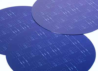 silicon wafer to change its electrical properties. In contrast to thermal diffusion, which uses high temperatures to drive the dopant into the silicon, Tong's method uses a fibre laser to inject a narrow beam of light into the wafer.
To dop a silicon wafer, the first step is to prepare the wafer for the laser process. The material must be warmed up before the laser application to reduce thermal stress in the wafer. Next, the laser is passed over the substrate at 0.3 m/min at 40% of its maximum power. Once the laser passes through the wafer, a thin layer of Al is deposited on the surface via thermal evaporation.
The laser's CO2 emission causes thermal gradients with varying geometrical profiles. The heat from the laser causes the constituents of the fibre core to rearrange themselves. This process creates a travelling melt zone, which recrystallises the material into a variety of structures. The authors show that in-silicon III-V compounds are formed, with parallel semiconductor layers forming in the core.
During subsequent processing, the gradients are applied to determine the geometric distribution of the constituents upon solidification. The result is a higher concentration of the lower melting point constituent in the laser focus. The laser-induced thermal gradients allow for controlled translation of the liquid alloy along the fibre's core. It also allows the liquid alloy to solidify.
Another method to dop semiconductor materials is called gas immersion laser doping (GILD). This process is performed by immersing a thin silicon wafer in a gas containing boron atoms. The laser then causes localised melting and recrystallisation of the silicon wafer, causing boron atoms to diffuse into the molten sections. The result is a high-quality semiconductor junction.
This technique is possible because of the high purity of the silicon core. It can be performed under controlled temperatures of 4500 K cm-1. The laser spot size and translation rate can be adjusted to suit the target material. The laser spot size can be 1 mm wide.
Undoping a silicon wafer
Doping a silicon wafer is a fundamental processing step in semiconductor fabrication. This step changes the chemical composition of the semiconductor and changes the electrical properties. Without doping, silicon is a poor conductor with a high resistivity. Doping changes this characteristic by adding various chemical impurities to the silicon. The result is either p or n-type silicon, which contains electrons and holes as charge carriers.
To dope a silicon wafer, a boron-rich glass formation layer is first deposited on the silicon wafer. Then, the wafer is heated to a temperature of at least one hundred and twenty-five degrees centigrade. This temperature is maintained for a period of about twenty-five minutes, and during this time, boron is diffused into the silicon wafer. The amount of boron deposited on the wafer depends on the temperature and the concentration of the boron dopant.
This process can be performed on a silicon wafer at different temperatures. The temperature and the dopant source determine how long the doping process takes. For instance, an aluminum metaphosphate solid dopant source may require thirty-five to sixty minutes to reach a sheet resistivity of four to five ohms/sq.
The standard process for doping silicon wafers uses a gas based dopant called phosphorus oxychloride or phosphine at temperatures between 950 and eleven hundred degrees Celsius. This method causes phosphorus oxide to form on the silicon surface. The elemental phosphorus then diffuses into the silicon, reaching a controlled depth.
A second temperature is used to oxidize the silicon wafer. This temperature is lower than the deposition temperature to limit P2O5 evolution. The solid phosphorus dopant source may remain in the diffusion tube during the oxidation process. This temperature is a crucial factor when it comes to doping a silicon wafer.
Phosphorus is an excellent dopant, but you may have to be cautious with its use. This material is prone to oxidation and is a potential source of problems when used in semiconductor manufacturing.
Fabrication of custom silicon wafers
Developing custom silicon wafers requires specialized experience and expertise. Okmetic offers three decades of experience in wafer fabrication and crystal growth. Their R&D scientists and Customer Support Engineers work with customers to understand the challenges they face and develop solutions that meet those challenges. As a result, customers can count on custom silicon wafers that are designed to meet their exact specifications.
Wafer manufacturing consists of four distinct phases. First, the silicon ingot is cut into thin slices with a diamond-tipped saw. Then, the remaining wafers are etched with a mild acidic solution and polished to remove any rough edges caused by the saw. Each wafer is composed of 18 silicon atoms and has weak bonding along its cleavage planes. Next, the wedges are classified according to their planar orientation by a Miller index.
The resulting custom silicon wafers can vary in shape, size, and composition. For example, the thickness of the flats on the edge of the wafer is different depending on the type. Another variable is the type of n-type or p-type doping. If you're ordering a single-sided wafer, you can ask for a single notch to identify the p-type doping.
The last step of custom silicon wafer fabrication involves chemical etching. This process removes layers of surface material, including crystal damage and contaminants. This step produces a highly reflective surface. This step is followed by chemical and mechanical polishing. This polishing step involves the use of an ultra-smooth polishing pad and a solution that contains hydrofluoric acid.
Another important step in the fabrication of custom silicon wafers is the machining process. This process involves the removal of a thin seed crystal from molten silicon. After this, the seed crystal is extracted as a cylinder of monocrystalline silicon, which can be as long as two meters. This process can produce hundreds of custom silicon wafers. These custom silicon wafers can be used for manufacturing thousands of ICs.
Due to the complex nature of silicon, fabrication of custom silicon wafers requires specialized capabilities. Lam Research has invested heavily in these capabilities. The Silfex division of the company is the largest provider of custom silicon components. This team has state-of-the-art material growing facilities, CNC machining centers, and automated cleaning systems. These advanced manufacturing processes are aimed at producing high-precision silicon parts and contribute to the success of Lam plasma etch systems.