Patterned Sapphire Substrates (PSS) for UV LEDs
Patterned Sapphire Substrates
We, along with our partners, can fullfill all your PSS needs. Patterned Sapphire Substrates (PSS) are micro-patterned wafers used to fabricate Gallium Nitride (GaN) light emitting diodes (LEDS). PSS reduces the dislocation density in the GaN layer. This results in more efficient llight extraction while increasing the brightness.
Using Patterned Sapphire Substrates can significantly increase the light output of LEDs. Benefits include:
- Increased light emissions of active quantum well layers as the result of reduced epitaxial defect density.
-PSS reduces light loss due to the Total Internal Reflection (TIR) phenomena by enabling a photon scattering effect.
Get Your Patterned Sapphire Quote FAST!
Patterned Sapphire Substrate for Ultraviolet (UV) LEDs
Researchers have used several types of sapphrie wafer including:
- Flat (FSS)
- Patterned (PSS)
- Silica Array (PSSA)
To make Ultraviolet (UV) Light Emitting Diodes (LEDs).
Patterned Sapphire Wafers for R&D
The formation of LEDs on patterned sapphire substrates is the most cost-effective method for manufacturing such devices. These LEDs exhibit high-normalized electroluminescence intensity and high light extraction efficiency. In addition, patterned wafers reduce defect density and total internal reflection losses. These advantages are driving the adoption of nitride-semiconductor-based LEDs by manufacturers.
Currently, patterned sapphire substrates are most often used for the production of semiconductor GaN epitaxial light-emitting diodes. The use of patterned sapphire substrates in this process is increasing due to the varying chemical resistance of the material. The following section details the fabrication of a PSS with pyramidal patterns. The process is described in detail below. The fabrication process was completed by wet etching and plasma dry etching.
A patterned sapphire substrate has several advantages. First, the patterning improves light extraction  efficiency. Moreover, it reduces the dislocation density in the GaN layer and increases LED brightness. Second, patterned sapphire wafers have high reproducibility, which is important for LED applications. They can also be used for other electronic devices. Hence, they have many applications. The key is to find an application for these devices in the market.
The development of patterned sapphire substrates is expected to benefit the high-brightness LED industry. They will provide a common basis for research, production and sale of LEDs. In this way, they will serve as a bridge between the downstream and upstream LED industries. So, what is a patterned sapphire substrate? This article will provide you with a basic overview of how this material can be used in high-brightness LEDs.
Another advantage of patterned sapphire substrates is that they enable a greater variety of techniques. For example, CPSS reduces the area between the sapphire and AlN. In addition, CPSS allows for the creation of a wider variety of TDs. The researchers in this field are now advancing research in order to improve the quality and performance of patterned sapphire. With these advances, a broad range of new technologies is expected to emerge.
Various kinds of patterned sapphire substrates have been designed to improve light extraction efficiency. In addition to the polygonal pyramid pattern, a triangular-pyramid shape was found to be optimal. A crystalline sapphire substrate with a faceted shape is more transparent and therefore more durable. It is a better material than a plain one and is much more expensive. However, it is still the most cost-effective option.
The industry is dominated by LED chipmakers, which fabricate the PSS themselves. But sapphire substrate manufacturers are emerging as a niche. In addition, they are partnering with LED chipmakers to put patterns on their products. The majority of these companies focus on small diameter patterning. Only a few are now offering 6-inch products. In 2013, Rubicon Technology launched its first larger-diameter PSS.
The researchers prepared a series of different PSSAs in the laboratory. The cones were 2.8 um in diameter, with three-millimeter center-to-center spacing and two-um height. These PSSAs were prepared using the thermal reflow photoresist technique and an inductively coupled plasma etching process. These are a good alternative to silicon for a wide range of applications.
The improved crystal structure of these patterned sapphire substrates has improved the efficiency of light extraction and heat dissipation of the semiconductor lighting devices. The resultant crystalline-Sapphire LEDs have higher luminous efficiency than conventional Prisms, but they require more power. For this reason, a commercial Prism LED is a good alternative. Its luminous efficiency is much higher than a conventional PrismLED.
The high-density features of PSS are important for the performance of these devices. These chips are crucial in many fields, including medical imaging. With high-end LEDs, they need to perform well in the laboratory. Unlike conventional Prism, a PV-based patterned substrate is unique in its properties. Its features are highly sensitive, durable and flexible. If the PV is etched with a Prism, it can be processed into a crystalline silicon device.
The advantages of PVs on patterned sapphire substrates are not limited to LEDs. The crystalline defect density of PSPs is high and it is not uniform. The lateral overgrowth of GaN on PSS-based devices has the potential to improve the efficiency of these LEDs. The overall efficiency and energy consumption of these lights are also reduced, thanks to the enhanced PSS. A PCS is a low-cost solution for producing LEDs.
The other important driver for sapphire is its use in semiconductor production for the aerospace and defense industries. The way in which the market is divided is subdivided - subdivided, based on its wafer - subdivided size. A very important sector for this is aerospace, which is divided into thin, high-performance, transparent and ultra-thin layers because of its transparent armour. [Sources: 7]
As mentioned above, the density of the edge dislocation decreases with the growth of the GaN layer, resulting in a reduced FWHM value of 102%. This effect is interpreted as the result of the compressed hydrostatic load on the component, which the thin Ga N layer undergoes. When cultivated in sapphire with an aln buffer layer, lead generally dissolves to about 2% and lead to about 0.5%. [Sources: 2, 5, 8]
Figure 2 illustrates the effect of planar sapphire lead on the FWHM of the GaN layer and the density of the edge contortions. Figure 5 shows the effects of the formation of a thin GaN layer with an AlN buffer layer of about 1.5%. [Sources: 5]
The effect of planar sapphire lead on the half-life of the GaN layer and the density of the edge contortions of a thin Aln buffer layer. [Sources: 5]
In addition to increasing apparent light output, a number of manufacturers claim that epitaxial layers on patterned substrates are more efficient than those grown on bare sapphire substrates. The FWHM value of LEDs with pss is lower than that of LEDs on sapphire substrates, suggesting that crystal quality is significantly improved by using PSS. The high EL intensity increases by 91% compared to LEDs on planar spheres and by more than 100% in planars. [Sources: 4, 5]
The larger diameter of sapphire wafers has the potential to make the manufacturing process significantly more efficient, but also presents challenges for manufacturers. For example, the cost of a 2-inch GaN wafer is about twice as high as for an 8-inch GaN wafer. Given the high cost of high-temperature wet etching, LED manufacturers and sapphire wafer suppliers need to seriously consider this, especially given the significant cost difference between the two substrate types. [Sources: 0, 7]
If demand for patterned sapphire substrates continues, it may ultimately be helpful for Sapshire to use other high-temperature wet etching technologies, as existing materials other than Sapshire have an established supply chain. The sapphire technology market and the growth of this technology are further segments, divided into two major segments: the semiconductor industry and the consumer electronics industry. This report is divided by industry into semiconductors, photovoltaics, electronics, automotive, medical devices and other industries. [Sources: 1, 7]
In the last 18 months of the program, we investigated the use of a specially developed sapphire substrate patterned with C-tarpaulins. The epitaxial structure of the LED is a contrast sample used by conventional sapphire substrates (CSS) using low pressure MOCVD. LEDs (light-emitting diodes) and nitride - based LEDs growing on a structuring saPPHIRE substrate (Fig. 2). [Sources: 0, 3, 6, 9]
A photoresist array was used as mask layer to transfer the sapphire pattern by applying an inductively coupled plasma reactive ion etching system using reactive Cl 2 gas. The membrane was turned upside down in a steel bracket and manually peeled off the SAPPHIRE substrate. A thick PDMS top layer was covered with a centrifugal layer and applied to a thin layer of C-tarpaulins (1.5 mm thick). [Sources: 3, 8]
This process is similar to that used in the silicon industry to produce the wafers used as substrates. This process makes the use of high temperature, high pressure and high temperatures, which are standard today, superfluous. [Sources: 4, 8]
According to the literature [16], the use of patterned sapphire substrates would effectively reduce the contortion of the filaments. Defects related to the degradation of electrical power, such as defects in the electrical conductivity of the wafers, are rarely investigated. [Sources: 5]
This article proposes a method to reduce the impact of bat ejection on patterned sapphire substrates by selecting the appropriate wavelength measurements. Atomic force microscopy (AFM) offers the possibility to study force - microscopy in a variety of materials such as lead, copper, gold and silver. This method can be used in many applications, for example, in chemical reaction analysis [16, 17, 18, 19, 20, 21, 22, 23, 24, 25, 26, 27, 28, 29, 30, 31, 32, 33, 34, 35, 36, 37, 39, 40, 41, 42, 43, 44, 45, 46, 47, 48, 49, 50, 51, 52, 53, 54, 55, 56, 57, 58, 59, 60, 61, 63, 64, 65, 66, 67, 68, 69, 70, 71, 72, 73, 74, 75, 76, 77, 78, 82, 83, 84, 85, 86, 87, 88, 89, 90, 91, 92, 93, 94, 95, 96, 97, 98, 99, 100, 104, 105, 106, 111, 112, 113, 114, 115, 116, 12 Atomic force microscopy offers the possibility to analyze the sapphire substrate before epitaxial film growth. In addition, the pattern and PSS techniques are suitable for GaN epilayers that achieve high crystal quality in a single, continuous growth process. [Sources: 3, 6, 10]
Sources:
[0]: https://www.imtecacculine.com/sapphire_pss_wafer_etch_wet_vs_dry.html
[1]: https://compoundsemiconductor.net/article/91564/Rubicon_reveals_sapphire_plans/feature
[2]: https://www.nature.com/articles/srep03201
[3]: https://www.hindawi.com/journals/ijp/2014/796253/
[4]: https://sst.semiconductor-digest.com/2015/11/the-use-of-sapphire-in-mobile-device-and-led-industries-part-2/
[5]: https://cyberleninka.org/article/n/1182219
[6]: https://www.spiedigitallibrary.org/conference-proceedings-of-spie/9960/1/Reduction-of-batwing-effect-in-white-light-interferometry-for-measurement/10.1117/12.2236874.full
[7]: https://www.marketsandmarkets.com/Market-Reports/sapphire-semiconductors-market-391455.html
[8]: https://www.science.gov/topicpages/m/m-plane+sapphire+substrates
[9]: https://www.osti.gov/servlets/purl/1238367
[10]: https://parksystems.com/applications/electrical-electronics/display/156-surface-topography-considerations-of-patterned-sapphire-substrates-for-blue-green-light-emitting-diode
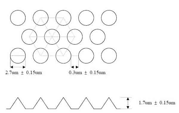
Below is just an example of PSS that we sell.
2" PSS with the following pattern specifications:
Pattern Pitch 3.0um ± 0.15um
Pattern Bottom 2.7um ± 0.15um
Pattern Space 0.3um ± 0.15um
Pattern Height 1.7um ± 0.15um