We are looking for a quote on two photomask layers for use in photolithography. These will be for a 6-inch wafer, so we would like a 7x7-inch mask. The smallest positive feature size is 20um, and the smallest negative feature is 15um. A film or chrome mask would be acceptable. We have the mask designs in .GDS format and can send them when needed. It would be great if we could get a quote and an estimated lead time.
Photomasks for Research & Production
What Photomasks are Used in Photolithography?
A PhD candidate in Biomedical Engineering requested the following quote:
Reference #272336 for specs and pricing.
Get Your Quote FAST! Or, Buy Online and Start Researching Today!
Photomasks Soda Lime and Fused Silica
A photomask is an opaque plate with holes or transparencies that allow light to shine through in a defined pattern. They are commonly used in photolithography. Lithographic photomasks are typically transparent fused silica blanks covered with a pattern defined with a chrome metal-absorbing film. Photomasks are used at wavelengths of 365 nm, 248 nm, and 193 nm. Photomasks have also been developed for other forms of radiation such as 157 nm, 13.5 nm (EUV), X-ray, electrons, and ions; but these require entirely new materials for the substrate and the pattern film.
Send us your specs today for an immediate quote!
What Are Some Photomask Applications?
Photomasks are placed on printed circuit boards, where they transmit precise images of the arrangement of integrated circuits to the printed circuit board. Photomasks used in the manufacture of integrated circuits are usually made of chrome layers deposited on quartz or quartz plates and then patterned by a photolithographic process. For each successive layer, different photo masking is used, and the material is deposited or removed in places that are not covered by the photomask image. [Sources: 2, 3, 9]
Each layer typically has one or more design rules associated with the specific layer created by the mask layout file. Each polygon in a layer can be converted into a mask pattern file, which is a layer of an integrated circuit. DRC tool creates an output file that contains a list of identified rule violations, typical of most mask and pattern generators. A grayscale application known as photomask (or photomask pattern generator, or even black and white mask generator) requires data that has the potential to be more detailed than the data available in a normal mask pattern generator. [Sources: 8, 10]
In this respect, the method for creating a three-dimensional structure consists of a binary halftone photomask that provides a photoresistic layer that covers the wafer. Next, a mask, defined as a variable intensity shade of gray, is transferred to a wafer coated with a thin film of photoreceptors (a type of silicon photovoltaics). This light is transmitted by a laser to produce three-dimensional aerial images. [Sources: 10]
After the mask pattern design is completed, the design is transferred to the photomask using the same method used for processing traditional binary photo masks as shown in FIG. After generating the three-dimensional structure of a binary semitone photomask on a semiconductor wafer (step 114), a photomask is used to map the pattern of the photomask on the semiconductors in the wafers (step 114). [Sources: 8, 10]
This material is sensitive to ultraviolet light, which is normally used for the exposure of photoresists. A glucose sensor in a contact lens is embedded with a binary halftone photomask to demonstrate the sensitivity of the photomask to a wide spectrum of wavelengths of light (Fig. 1). [Sources: 4, 5]
When a BHT photomask is used to create three-dimensional microscopic structures, it is possible to create a smoother and more linear profile in the object to be created. [Sources: 10]
If subpixels 21a and 21b are arranged on a plane and the gray plane has an associated plane, the open area of a single cell can be changed if a correction of the nonlinearity of the process is required. A separate photomask can contain a list of all compounds and contact layers that are formed by the diffusion step in the manufacturing process. Therefore, the mask layout files may contain one or more polygons drawn on the polysilicon layer that have not been explicitly shown, even if they are not explicitly shown. Photomasks can also be used to create features, dimensions and masks in a layout file that are compared with the design rules and technology files. For example, the photomask files may contain photomsks used to form polysilicon gates in an integrated circuit, or a separate photomask file may contain photomyzen photomenes used to form a polysilicon gate for an integrating circuit. [Sources: 8, 10]
A transparent photo mask is a template that is transferred to a photosensitive polymer known in lithography as photoresistent, which is called photoresistent polymers by photoreceptors. The empty binary photo masks are preferably standard photo masks made of chrome or quartz, coated with a layer of photoresist (51). [Sources: 7, 10]
The mask layout database is then converted into several photomasks, also known as mask reticles, which can be used to map the integrated circuit. In step 110, the photomask data file is used in the lithography tool to create the photomask layer of the integrating circuit (110). [Sources: 8]
The size of the photomask is not tied to the wafer size; for example, if the lithography tool is exposed to a 300 mm by 200 mm wafer, a 6 inch photomask can be used. In this respect, the three-dimensional structure consists of two layers: a hole pattern and a layer of photomask lying on the surface (essentially linear surface), which corresponds to binary (semitone) photomasks generated by light aerial images. The pattern of a photomask must be demagnetized and thus projected onto a surface with a diameter of at least 1.5 mm. In general, hole patterns on awafer often have an almost circular shape and are the same size as holes in a single layer (2.2 mm x 2 mm) or larger (3.1 mm). [Sources: 0, 1, 9, 10]
You will understand that the threshold and dose of light exposure can determine the photoresist layer used in the photolithography process. It can be used for simple description to describe the elements and the features shown in the figure. [Sources: 6]
In traditional optical lithography, a fully resolved pattern is etched onto a binary photomask and transferred to the wafer by exposure with an exposure tool (e.g. stepper). When used with a lithographic tool for wafers, the light pattern transferred by the photomask is applied to the photoresist film of the silicon wadding. A thin absorber layer is placed on the substrate, which can block the exposure of light with the wafer lithograph tool. The holes in the pattern are designed to absorb a light dose of up to 1.5 micrometers (0.1 micrometers) per second. [Sources: 0, 9, 10]
Sources:
[0]: https://www.freepatentsonline.com/y2009/0077524.html
[1]: https://www.ptb.de/cms/en/ptb/fachabteilungen/abt5/fb-52/ag-522/masken522.html
[3]: https://www.wisegeek.com/what-is-a-photomask.htm
[4]: https://www.nature.com/articles/s41467-020-14439-1
[6]: https://patents.google.com/patent/US20150050584A1/en
[7]: http://lnf-wiki.eecs.umich.edu/wiki/Mask_making
[8]: https://www.google.com/patents/US20020152453
[10]: https://patents.justia.com/patent/20030138706
What Substrates are used for Photomasks?
 There are two main types of substrates for a photomask. Glass and quartz are the most commonly used. These materials are coated with a thin film of photoresist, which is light-sensitive. When exposed to light, the exposed photoresist is washed away and the Chrome is exposed. Then, the photomask is developed and etched. This process leaves the mask with a series of holes that allow light to pass through.
A photomask is a thin layer of masking material supported by a thicker substrate. This layer absorbs light at varying intensities and is patterned with a custom design. Light passes through the substrate and transfers the pattern. Photolithography is an important process used in the manufacture of digital devices. If you are planning to use a photomask, it's important to choose the right substrate.
A photomask is an opaque pattern supported on a larger substrate. Using a glass or film substrate will help to ensure an accurate result. Depending on the size of the image you want to produce, you can choose between a glass or a film substrate. You can also choose from various kinds of metals and other materials for your photomask. The metal of your photomask is the most common choice for photomasks, but a glass or a film substrate will work as well.
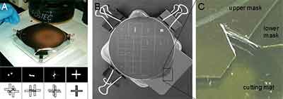
Chrome Photomask for Cancer Research on Soda Lime Wafers
A researcher asked for the following:
Patterned Area: 19mm x 19mm Pattern: Concentric Circles Height: 50μm Line width:  25μm Period: 50μm master will be used to mold PDMS cured onto a metal substrate for subsequent stem cell/cancer research. For a soda lime, inexpensive but durable – researcher plans on coating the master with a fluorocarbon resist to allow for easy extraction from the PDMS (leaving no residue). Cut in cross-section, the master should look like a square-wave. The resulting PDMS pattern (ie the resulting high sections of the pattern), when exposed to cells in cell culture will be as flat as possible.
This is a chrome on glass photomask. The pattern is etched into the chrome surface.
This is for a photomask. The original request for quote suggested that you required a photomask that would be used to create a mold.
UniversityWafer, Inc. Quoted:
Because it is a photomask, the depth of the etching is normal for a photomask – just 120nm thickness of chrome.
3" Chrome Photomask PRICE $Please contact us.
SKU: H03-LC-SL60-CL1-DTP- -S5-IS-
Base Material
Soda Lime Glass (0.063" - 1.6mm)
Resolution
Class 1......64k dpi.....
Min CD (smallest feature)
25um
CAD Format supplied
DTP (Corel / AI)
Polarity (see description)
Positive - Right Reading Chrome UP
Production Schedule
5 days +
Inspection Requirements
Standard Inspection
Checkplot Required
PDF Checkplot
YOUR Drawing Number / CAD filename
0.75 in 76 concentric circles 50 micron
How Big is The Photomask Market?
If you are looking to create a high-quality photo-mask, you need to understand the fundamentals of semiconductor processing. As demand for Semiconductor Photomasks rises, so do their prices. In order to keep up with demand, suppliers must focus on delivering products as fast as possible. This shortage will only intensify in the coming years, so you should take steps to minimize your production costs while maximizing your yields.
To understand the market and potential future growth, you should first understand the fundamentals. In order to create a photomask, it must be made with opaque film and substrate. Then, it must be cleaned and etched. Once the blank is ready, it is inspected for defects. If any material is missing, it is covered with a protective membrane, called a pellicle. This is used to protect the mask from contamination and falling particles.
Semiconductor Photomask market is segmented by region, manufacturer, type, and application. The report also studies the trends and opportunities in each segment to determine which companies will dominate the industry. It also examines the future of the market by examining the competitive landscape. By product, the industry is divided by the end user, and type. This segmentation is used to identify the leading players in the Semiconductor Photomask market.
The semiconductor photomask market is dominated by companies from Japan, South Korea, and the United States. This technology can be used in several industries, including solar cells, integrated circuits, and mobile devices. Aside from the various applications, the market for Semiconductor Photomask is growing at a rapid rate. The growth potential of the market is expected to be impacted by the global economic recession, but the industry will rebound in 2021, with a 3% to 5% CAGR.
The semiconductor photomask market is a lucrative industry. According to the SEMI, the semiconductor photomask market is valued at over $4.2 billion. The technology is used in a wide range of applications, including the manufacturing of advanced components and electronics. The growth of this market will depend on the needs of different industries. The technology will continue to evolve and the need for more efficient production will increase. This will drive the demand for photomasks.
The semiconductor photomask market has reached a record high in 2018. SEMI estimates that the market will reach more than $4 billion by 2020. It is expected to grow at a steady pace in the Asia-Pacific region, driven by demand for advanced technologies and the increased use of advanced materials in the semiconductor manufacturing process. The market for semiconductor photomasks has a wide geographical spread. By geography, Taiwan has the largest market in the world.
The market for Semiconductor Photomasks is highly competitive in terms of its size. It has many advantages and disadvantages, and is widely used in a variety of applications. The most popular ones are silicon-based ICs. Despite its complexity, however, these devices are a valuable investment in the electronics industry. They will increase the volume and performance of devices, and increase efficiency and reduce overall costs. So, the industry will grow at a steady pace in the coming years.
The Semiconductor Photomask market is expected to expand at a steady rate in the coming years. The market is projected to experience a decline in 2020 due to the global economic recession, but will rebound in 2021, growing at a 3% to 5% CAGR during this period. The key growth drivers for the Semiconductor Photomask market include the growing popularity of consumer electronics and the adoption of automated systems across various industries.
Several factors drive the semiconductor photomask market. For example, the technology involved in the production of semiconductors is highly advanced, so the need for a high-quality photomask is an essential aspect of a modern semiconductor. In addition to this, the market is highly competitive and will likely grow at a rapid pace in the coming years. Therefore, a high-quality image of a Semiconductor Photomask can significantly impact a company's sales and profitability.
A semiconductor photomask is a flat, 6 inch square plate that is coated with an opaque, transparent, or phase-shifting pattern. This design is used to define the layout of one layer of an integrated circuit. A semiconductor photomask can cost anywhere from $250 to $100,000. The design is similar for a wide variety of CAD software and a variety of applications. A good-quality mask will help you achieve the best results in the manufacturing process.
What is a Semiconductor Photomask?
The term "semiconductor mask" is used for a variety of devices. A semiconductor mask is an integral part of any device, from solar cells to microwave-frequency integrated circuits. A typical fabricated semiconductor mask is composed of two layers, called the frame and the film. The frame contains test marks and metrology marks, and is typically built by the fab after it has known the primary pattern. The process also involves etching. The most common etching method uses plasma, which sprays ions on the frame and the substrate. This removes any residual resist.
A semiconductor mask is made by exposing a latent image of the design data into a photoresist. This photoresist contains a layer of material called a resist, which is engineered to withstand the etching process. The resistance of the resist must be slower than the rate of removal of the underlying Chromium. Either plasma or liquid chemistry is used to perform the etching process. After the etching process, the remaining resists are removed from the mask. This process is called stripping, and it usually takes place in a nanostrip that is heated to 60 degC.
A photomask is a transparent film used to create a pattern on a semiconductor device. A photomask is often used to print a pattern, but a photomask is an optical device that can be printed directly onto a semiconductor chip. A mask is a type of optical device, and it can be made with or without a silicon film. It is made of multiple layers of resists, and each layer is etched one by one to create a unique pattern.
A photomask can be made from photoresist, and it exposes a latent image of the design. In the past, the masks were made from rubylith, and multiple copies of the design were stamped on one piece of paper. The process became increasingly complicated as the complexity of the IC grew, and large patterns were cut to fill the walls of a room. Then, they were optically shrunk onto a photographic film.
As transistors become smaller, photomasks are increasingly complicated. The photomask is used to transfer the pattern from a photolithographic process to a silicon wafer. It is important to ensure the correct photomask pattern for high-revenue chips, as even the smallest defect can affect the performance of the silicon device. It is vital to check the quality of a photomask before it is used.
A semiconductor mask is used to create photoelectrochemical processes. Its manufacturing process has several steps. First, the chipmaker designs the IC and creates a file format. Next, the photomask facility fabricates the photomask using the file. The photomask is then placed inside a lithography scanner. The etching process requires the mask to have a low resistance.
A semiconductor mask is a thin, opaque film that transfers a pattern to a semiconductor device. It is a key component of a modern electronic device. A photomask is also used for solar panels. In addition to the photomask, a silicon chip can be manufactured using the same process. A transistor is one of the most common uses for a semiconductor. It is made up of many layers, including a dielectric layer and a resistive film.
A photomask is a mask that is designed to absorb a discrete wavelength of light. The most common wavelengths for this process are 193nm (ArF DUV), 248nm (KrF DUV), and 436nm (g-line). The photomask is a type of semiconductor mask that is made of a polymer, which is a transparent material.
A photolithography mask is a transparent film or plate that allows light to shine through in a defined pattern. It is commonly used in the manufacturing process of semiconductors. It is usually a transparent film or plate. A reticle has an image of the desired pattern. The entire wafer must be exposed to the laser in order to make the desired device. This process is called a photolithography. There are several different types of reticles available.