We would appreciate if you would send a quote for 3 x 100 mm CZ single-side polished Si p-type (Boron doped) wafers with a Phosphorous diffusion forming a junction. Additional specs provided upon request.
Solar Silicon Wafers 125mm & 150mm Psuedo Squares
Silicon Wafer Improve Light Absorption
Only limited work has been done with Silicon wafer based solar cells using Ag or Al nanoparticles because of the fact that the thickness of Si-wafer cells absorbs nearly 90% of sunlight at higher bandgap19,20,21,22,23,24,25,26,27. Despite calculations, efficient light absorption, including infrared parts of the solar spectrum, is feasible with even relatively thin (100-150 mm) wafers, if the wafer surfaces are simply texturized, combined with use of carefully designed antireflective coatings and back-surface mirrors.17 In practice, the recombination of carriers within the silicon may be affected, and may also dominate, due to the presence of defects or foreign impurities.
We propose the use of silicon wafers to improve light absorption and improve the conversion efficiency of silicon solar cells. The gap between the current state of the art in silicon photovoltaics and the next generation of solar cells has widened due to the success achieved in the development of highly efficient silicon PV cells in recent years.
Get Your Solar Wafer Quote FAST!
Thin Float Zone SIlicon for Solar Applications
Researchers have discovered that the thinner a silicon wafer is the more efficient.
Ask for Item#253540
2” and 3” diameter, float-zone, Si(100), n-type 1-5 Ohm-cm 20 microns thick
Solar Wafers with PN Junction
Researchers asks: I was just wondering whether the “Solar” products have a PN junction already (i.e. product ID 2920). If not, do you stock any products with a PN junction?
UniversityWafer Answer:
1) For solar application, P/N junction is typically made with a diffusion process. We do have a diffusion facility capable of creating junctions on wafers with diameter up to 4". Please let us know if you are interested in going into the project on a smaller diameter wafers.
2) We also have Si wafers with P/N junctions created by silicon on silicon epitaxial deposition method. Please ask for our inventory.
Silicon Solar Wafer Availability
A researcher asked the following:
I want 4 inch silicon wafers p-doped to ~10^15-10^16 cm^-3. The doping concentration is a bit flexible as long as it's not above 10^18 cm^-3. We don't have a strict requirement of thickness but ~200 um would be better. But the top surface has to be heavily n-doped to form n+ emitter. This is the minimum requirement for our wafers. In addition, if it is possible to heavily p-dope the back surface of the wafer to form ohmic contact, that would be great as well. If this kind of wafer is readily available at University wafers, we would like to order quickly. If it is not readily available but possible to prepare within a few days, please let me know that as well. Depending on the price per wafer, we will order a few.
UniversityWafer Answer:
We offer:
Item Qty. Description
GX82. 25 Solar cell silicon wafers, per SEMI Prime, P/P 4"Ø×300±25µm,
P/B[100]±0.5°, Nc=(3.05-1.50)E15/cm³, Ro=(5-10)Ohmcm,
Both-sides-polished,
With Diffused Phosphorus layer ~1 µm thick, of Nc=(3-10)E18/cm³, Ro~(0.005-0.012)Ohmcm}
SEMI Flats (two),
Sealed in Empak or equivalent cassette,
Note: Please see the pictures for the surface after process.
Price: $ Please contact us.
Photo of the wafer after our diffusion process. We expect a similar surface now.
Replacing N-Type With P-Type Wafers For Silicon Heterojunction Solar Cells
Silicon heterojunction solar cells (SHJ), which consist of N-silicon wafers (Cz), have aroused growing industrial interest. The low efficiencies can be achieved by using low-cost, high-efficiency silicon cells, and the cheap silicon can also be used to form SH J cells.
The work uses a Monte Carlo simulation approach that allows us to take into account uncertainties regarding the performance of different types of silicon wafers and their properties. We identify the most important factors influencing commercial comparison between wafer types.
N-type wafers achieve the same efficiency as SHJ solar cells with a different silicon wafer type. Our analysis suggests that the p-types of SHj solar cells should be at least twice as efficient as their n-types. This work represents a new approach to the production of SH-Joules per square centimeter (n - p) of SH-J cells from p- type wafer waves.
How Electrons Are Released in Solar Cells
Electrons are released in solar cells when light hits them. In a typical PV cell, the energy from the light falls on a silicon atom that is made up of three shells. The first two shells are completely full, while the outer shell has only half as many electrons. When the light hits the cell, the excited atoms flow into the holes, filling them with free-floating hydrogen ions. The movement of the holes and the free-floating ions causes the electrical current to flow, generating electricity. This process is known as the photovoltaic effect.
When light strikes a solar cell, the electrons are released into the air. These free electrons flow into the circuit, where they get energy from the photons. Once they have used all of their energy, they are released back into the cell and repeat the cycle. The energy in the cell is then transferred to an external load. The resulting voltage will be the output of the PV. A PV cell can produce electricity from the light it receives.
When the sun shines on a solar cell, the electrons in the cell are "knocked loose." These free electrons dart around the silicon layers, useless for electricity generation until they reach the junction between the two types of semiconductors. Once there, the electric field pushes the electrons upwards and slingshots them towards a metal conductor strip. A photon is converted into electricity when the light strikes the semiconductor.
To generate electricity, the electrons are released from the silicon cell. They move through a conductive wire and recombine with a hole in the p-type side. The remaining electrons in the n-type layer are transferred to an electrode connected to an external load. Once released, the solar cells become useful. It's important to understand that sunlight is an important source of energy for solar cells.
When the sun's light hits a solar cell, electrons are freed from the semiconductor. The electrons are free to move from one layer to another, which is why they can't be released from the same cell. This is because they seek out the lowest resistance and the most efficient path. Unlike in ordinary cells, the electrons of the solar cell have to cross through the entire circuit to reach the next layer.
In PV cells, electrons are released from the semiconductor material and travel through a metal conductive plate on both layers. The electrons leave the cell as an electric current, which can be used to power a load. This electrical current is released from where are electrons released in solar cells. The amount of electricity produced depends on the amount of sunlight. For example, if the cell is exposed to a bright light, it will release a negative charge.
An electrochemical process creates a current in a cell. An electron can move through the semiconductor by receiving photons. The photons that arrive in a silicon solar cell "excite" it and move into the conduction band. Then, the electron is released from its valence band and moves into the conduction band. This is a hole. When the electrons are free, they can move around freely, but they cannot exit the semiconductor.
As light hits a layered solar cell, electrons are free to move randomly. The electrons closest to the p-n junction cannot return in the opposite direction. The excess electrons flow in the n-layer and create a charge imbalance. However, the charge imbalance is corrected by releasing the electrons. Then, the energy is used in the home, the rest of the electric grid, and in a wide range of other applications.
Light strikes a layered cell, and electrons are free to move randomly in the space between the layers. Then, the light strikes a crystalline silicon molecule. An incoming electron has a certain amount of energy, which is called the band gap. This band gap is the place where the electrons travel. As light passes through the layered cell, it absorbs the energy. This makes the energy available in the n-layer.
What are Types of Solar Cell Wafers?
The solar cell is a semiconductor that can convert sunlight into electricity. The structure is made of a stack of solar cells with different band gaps. Each cell absorbs photons with the appropriate band gap. A solar cell that uses a thin film of a semiconductor can be a cheap way to generate power. The process is scalable and can be scaled up to commercially viable levels. However, it requires significant investment and technological know-how to reach its potential.
The most common type of solar cell is a monocrystalline silicon panel. These cells are  typically composed of a single-crystal substance. This makes electrons move more freely. In addition, they have a distinctive pattern of small white diamonds. Typical commercial solar cells have a fill factor of 0.70, while grade B cells are usually between 0.4 and 0.7. A monocrystalline panel will have fewer internal losses than a multicrystalline panel.
Standard industrial silicon cells are capable of achieving higher efficiencies than other single-junction devices. These high-quality devices also offer better durability, with modules lasting for more than 25 years with little long-term degradation. Moreover, these panels are highly durable, with few signs of deterioration. They are also environmentally friendly, as they require no maintenance. And since the sun does not emit carbon dioxide or other pollutants, they can be a reliable source of energy.
While silicon is a very popular material for solar cells, there are many other materials that can be used in the construction of these panels. Besides silicon, perovskite is also a common alternative to silicon, especially for the manufacturing of solar cells. This material is characterized by low maintenance and easy installation. It is also a great alternative to traditional solar panels, as it is more durable and does not need regular maintenance. If you want to build a high-efficiency panel, you should look for a high-quality solar cell.
There are two kinds of silicon cells: n-type and p-type. The n-type silicon cells are positively-charged and are based on phosphorus. The n-type cell is the most efficient, as it achieves a high efficiency of up to 30%. Unlike p-type cells, n-type solar cells are highly expensive. For this reason, a crystalline silicon cell is much more expensive than a p-type one.
In the solar cell, a single solar cell has a surface area of about 256 square centimeters. A solar panel is made up of dozens of these cells. In a single solar panel, a single solar cell can contain hundreds of thousands of cells. This technology has been developing since 2009 and is a great option for home and commercial applications. A typical PV panel can produce over one megawatt of electricity per day.
One of the most common types of solar cells is made from n-type CZ silicon. These cells have an excellent surface passivation property and are often coated in a thin layer of silicon nitride. Some solar cells have textured front surfaces to increase the amount of light that reaches the wafer. The n-type silicon cells are most expensive. They need to be made of a material with a high fill factor.
The cost of solar cells varies greatly. Typical solar cells are very costly. In the long run, a PV system will be more affordable than the conventional method. If it's possible, consider a solar panel with n-type silicon for your home. The technology is more expensive but can provide electricity for years. It's also good for the environment, as it's free from harmful emissions. For more information, read Energy Basics
To make a solar cell, two layers of p-type silicon are placed side by side. The n-type silicon has an excess of electrons while the p-type has an excess of positively charged holes. The n-type solar cell has more electrons. A p-type solar cell has a low fill factor. Thus, it has a higher fill factor. The higher the fill factor, the more stable it is.
Graphene aerogel is also a component of solar cells. It is added to the hole transport layer under the perovskite absorber layer to act as a moisture barrier. This improves the conversion efficiency. The n-type solar cell also features a surface-textured surface. It is very similar to the monocrystalline version. So, the only difference is the shape. There is no crystalline structure in the polycrystalline ones.
Solar Silicon Wafers
Summary of Solar Cell Production, and Limiting Efficiency of Silicon Solar Cell
Limiting Efficiency
It has been well established that the limiting efficiency of single crystals falls at about 29% [Swanson] this limit was established in the seminal work by Tiedje. In figure 1 we can see this limiting efficiency as a function of solar cell thickness. In this diagram, the peak efficiency is shown to be 29% with a thickness of just under 100µm.
Typical production solar cells achieve about 20% efficiency, while the best laboratory efforts have achieved about 25% [Swanson]. Green provides an excellent summary of the current progress of high-efficiency single-crystal silicon solar cells, and reconfirms the 29% limit established by Tiedje.
Production Process.
The process of manufacturing solar cells from single crystal p-type silicon wafers is detailed below. This is the generalized method used based on a number of sources. It should be noted that different companies have different patented, and trade secret processes for each of these steps, but the steps remain the same.
Texturing:
After an initial cleaning procedure, the wafer is textured to create pyramid-like structures on the surface of the silicon. This causes incoming sunlight reflected off of one pyramid to bounce into other pyramids on the surface improving the overall sunlight absorption rate.
N doping (usually Phosphorous):
A variety of methods are used to dope the top surface of the P-type wafer to create N-type regions. This process (typically gas diffusion in a high-heat furnace) creates the critical p-n junction which forms the permanent electrical field.
Edge diffusion cleaning:
The doping process causes the phosphorous dopant to diffuse to the edges of the wafer, if this excess dopant was allowed to remain it would cause short circuiting between the positive and negative contacts of the solar cell. The excess dopant is removed by an acid-etching procedure.
Anti-reflective coating
The wafer is then given an anti-reflective coating, usually silicon nitride, to improve absorption.
Screen printing of front and rear surface contacts
In the final step of the production process, front and rear surface contacts are screen printed onto the surface of the wafer to create the positive and negative contacts of the solar cell. The solar cells are then ready to be wired together to create solar panels.
References
1.) Tiedje et al; Limiting Efficiency of Silicon Solar Cells: https://optoelectronics.eecs.berkeley.edu/ey1984ieeeed315.pdf
2.) M.A Green; Progress and outlook for high-efficiency crystalline silicon solar cells https://144.206.159.178/FT/957/22841/412931.pdf
3.) Swanson, R.M; Approaching the 29% limit efficiency of silicon solar cells
4.) Solar Cell production process https://www.photonics.com/Article.aspx?AID=40098
5.) Solar cell production video: https://www.youtube.com/watch?v=TRATu_wEgAY
6.) Solar Cell production video: https://www.youtube.com/watch?v=fZ1SC-vUe_I
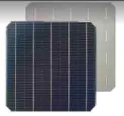
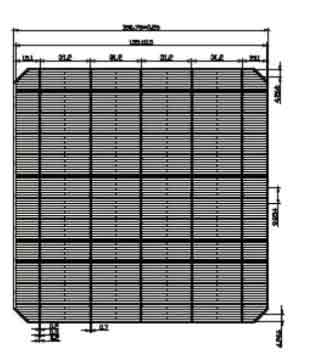
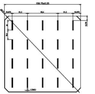
156 Mono Solar Cells
We have the following 156.75mm x 156.75mm +/-0.25mm substrates.
| Dimension | 156.75mm x 156.75mm + 0.25mm |
| Diagonal | 210mm + 0.5mm (Round Chamfers) |
| Thickness | 200um + 20um |
| Front | Anisotropically texturized surface and dark silicon nitride anti-reflection coatings |
| 0.7mm silver busbars | |
| Back | local aluminum back-surface field |
| 1.7mm (silver/aluminum) discontinuous solderng pads |
| Production and Quality Control |
| Precision cell efficiency sorting procedures |
| Stringent criteria for color uniformity and appearance |
| Reverse current and shunt resistance screening |
| ISO9001, ISO14001, and OHSAS 18001 certificated |
| Calibrated against Fraunhofer ISE |
| Electrical Performance | ||||||
| Efficiency Code | 216 | 215 | 214 | 213 | 212 | 211 |
| Efficiency | 21.6 | 21.5 | 21.4 | 21.3 | 21.2 | 21.1 |
| 5.28 | 5.25 | 5.23 | 5.2 | 5.18 | 5.16 | |
| Max. Power Current | 9.29 | 9.26 | 9.24 | 9.22 | 9.2 | 9.19 |
| 9.76 | 9.73 | 9.72 | 9.69 | 9.67 | 9.66 | |
| Max. Power Voltage | 0.568 | 0.567 | 0.566 | 0.564 | 0.563 | 0.562 |
| 0.667 | 0.666 | 0.665 | 0.664 | 0.663 | 0.682 | |
| Efficiency Code | 210 | 209 | 208 | 206 | 204 | 202 |
| Efficiency | 21 | 20.9 | 20.8 | 20.6 | 20.4 | 20.2 |
| Power | 5.13 | 5.11 | 5.06 | 5.03 | 4.98 | 4.94 |
| Max Power Current | 9.16 | 9.14 | 9.12 | 9.07 | 9.03 | 8.99 |
| Short Circuit Current | 9.64 | 9.62 | 9.6 | 9.56 | 9.52 | 9.49 |
| Max Power Voltage | 0.56 | 0.559 | 0.557 | 0.555 | 0.552 | 0.55 |
| Open Circuit Voltage | 0.661 | 0.66 | 0.658 | 0.656 | 0.654 | 0.652 |
| Temperature Coefficients | ||||||
| Current Temp Coefficients | 0.04%/C | |||||
| Voltage Temp Coefficients | -0.32%/C | |||||
| Power Temp Coefficients | -0.42%/C |
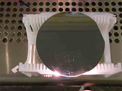
Creating Junctions on Silicon Wafers
UniversityWafer, Inc. and partners have a diffusion facility capable of creating junctions on wafers.
A researcher client asks the following:
UniversityWafer, Inc. Quoted:
Diamter 100mm CZ single-side polished Si p-type (Boron doped) wafers with a Phosphorous diffusion forming a junction
Contact us for pricing
What Are the Advantages and Disadvantages of Silicon Solar Cells?
Despite the fact that silicon solar cells are considered to be one of the best types of solar cells, there are many factors to consider before deciding whether or not it is the right choice for you. These factors include how the cells are manufactured, the quality of the cells and the price.

Monocrystalline silicon
Compared to other types of solar cells, monocrystalline silicon solar cells offer the best performance rates and power outputs. However, they are also the most expensive.
Monocrystalline silicon solar cells are formed from pure silicon, which is then sliced into thin wafers. The wafers are then polished and cooled. They are then assembled in rows and columns to form a monocrystalline panel.
The term "monocrystalline" refers to the fact that the cells have a single crystal lattice structure. This lattice structure provides more room for electrons to move, and allows the cell to convert more sunlight into energy. The average conversion efficiency of monocrystalline solar cells is 1% higher than that of polycrystalline solar cells.
However, because the manufacturing process is complex, the cost of producing monocrystalline silicon cells is higher. This is a factor that must be considered when considering which type of solar cell to use.
Monocrystalline solar cells are also less wasteful, which means that less space is needed to produce the same amount of energy as a polycrystalline panel. This is one reason why monocrystalline solar cells are usually used in larger installations.
In general, monocrystalline solar panels have better performance rates in low light conditions than a similar rated polycrystalline solar panel. However, they also have a disadvantage when it comes to temperature. The performance of monocrystalline solar panels is greatly diminished when it is warm, while polycrystalline panels are more effective when it is cold.
The maximum efficiency of a monocrystalline silicon solar cell is a mere ten percent, while the maximum efficiency of a polycrystalline solar cell is about twenty-five percent. As the materials and manufacturing process develop, new types of cells will be introduced.
In general, single crystalline solar cells have good stability, and a long service life. They also have a lower cost than polycrystalline cells. However, they also have lower efficiencies.
Monocrystalline silicon solar cells can be recycled. They are usually used in solar rooftop systems, and they are also widely used in batteries and electronics. They can also be used for charging cameras and batteries.
Polycrystalline
Unlike mono-crystalline solar panels, polycrystalline solar cells are made from multiple pieces of silicon. They can be synthesized in a variety of ways, including by high temperature chemical vapor deposition or by cooling liquid silicon with a seed crystal.
Regardless of the method used to create the cell, it's important to remember that the polycrystalline cell isn't a complete solution to the problem of creating a solar cell. The advantages of polycrystalline silicon solar cells include their ability to reduce the amount of greenhouse gases and other pollutants that result from burning fossil fuels, as well as their ability to reduce the costs of manufacturing solar cells.
Unlike mono-crystalline panels, polycrystalline panels are easier to manufacture. They require a smaller quantity of silicon than mono-crystalline cells, which saves manufacturers money and makes the process less costly. Polycrystalline panels are also less expensive to buy, which helps keep prices down.
Polycrystalline solar cells also have a number of other benefits, including a high degree of efficiency. The efficiency of polycrystalline cells ranges from 13% to 16%, and they are expected to increase over the next few years. Some newer experimental models are reported to reach the 50% efficiency mark.
Thin film solar panels are an alternative to mono-crystalline solar cells. These panels are thinner and lighter, making them more flexible and less expensive. They also perform better in high heat conditions. However, they are less efficient than crystalline silicon panels.
Mono-crystalline solar panels have a number of advantages, including their durability. They also look great. They have a classic black look. But the biggest advantage of mono-crystalline solar panels is their efficiency. They tend to outperform polycrystalline panels when it comes to temperature coefficient. This tells you how much your power output decreases for every one degree your panel's temperature increases.
Although mono-crystalline panels are more expensive, they have proven their worth over the years. They are also better for the environment, as they use less silicon. They also last longer than their polycrystalline counterparts. Ultimately, you'll find that the choice between poly- and mono-crystalline solar cells is a personal one.
Thin-film
Compared to traditional solar panels, thin-film solar panels have a lot to offer. The panels are lightweight, bendable, and they require less silicon to produce the same amount of electricity. They are also less prone to cracking. They are great for use in school systems, solar farms, and corporate solar power. They can also be installed on curved surfaces, a feature that can be beneficial for building-integrated photovoltaics (BIPV).
Thin-film solar cells are made from hydrogenated amorphous silicon (a-Si:H) based layers, which are deposited on a flexible substrate material. These layers are then placed on electrodes. In some applications, a back reflector is also added to prevent light from escaping the rear of the cell.
Thin-film solar cells are not as efficient as rigid photovoltaics. This is because newer materials have a lower number of charge carriers collected per incident photon. The newer materials also use less cadmium, which is toxic.
There are three types of thin-film PV cells that are viable today. These are cadmium telluride (CdTe), amorphous silicon (a-Si), and copper indium gallium selenide (CIGS). The CIGS cells are promising because they use a lower amount of cadmium and provide competitive efficiencies to silicon panels.
The cadmium telluride cells have a peak efficiency of more than 22.1% and are one of the most widely used thin-film solar technologies. They are less expensive than silicon thin-film cells and have a quickest payback time.
Amorphous silicon panels are the second most widely used thin-film PV technologies, and they are used for small load requirements. They are less efficient than monocrystalline or polycrystalline solar panels, but they are better for use in low light. They are also incredibly flexible, making them ideal for use in curved surfaces.
These cells are produced using a variety of inorganic and organic materials. Most technologies use organometallic compounds. Other technologies include dye-sensitized and quantum dot. However, the majority of these technologies are still in development and have not yet been commercialized. They are classified as emerging photovoltaics by the National Renewable Energy Laboratory.
Among thin-film PV cell technologies, copper indium gallium selenide (CIGS) is the leader. It is less toxic than cadmium telluride and uses a smaller percentage of cadmium.
Perovskite
Compared to silicon solar cells, perovskite solar cells are cheaper to produce and have a shorter life span. The efficiency of perovskite solar cells is also higher. Compared to silicon solar cells, perovskite cells can be thin and flexible. They are also less toxic. In addition to that, they can be produced on a large scale.
Perovskite solar cells are based on the mineral calcium titanium oxide. Calcium has a similar ionic radius to lead and is an inexpensive material. It also has high bandgap. This means that light-generated electrons and holes can travel a long distance. The high mobility of the charge carriers means that the device can extract maximum energy from the sunlight.
Perovskite solar cells have the potential to replace silicon-based solar panels. However, there are still many challenges to overcome. These challenges are discussed in this chapter. These challenges include stability, long-term efficiency, and cost.
The performance of perovskite solar cells is affected by the size of the bandgap. This bandgap is the amount of energy that is required to push an electron to a higher energy level. It is important to reduce the bandgap in order to improve the performance of the device. This is achieved by replacing the organic cation with an inorganic cation.
Although there are numerous challenges to overcome, the technology has made significant progress. Perovskite solar cells have exhibited improvement in efficiency from 3.8% in 2009 to 22.7% in 2014. There are also concerns about stability. However, this could be alleviated by improving the quality of the materials.
Perovskite solar cells also have the potential to solve energy poverty. Over 940 million people worldwide do not have access to electricity. In addition, these devices are affordable and flexible. These characteristics of perovskite solar cells could lead to a global revolution in the solar industry.
In addition to that, the devices can be used on surfaces that are not suitable for silicon solar panels. They can also be deposited using low-temperature methods. This method can help reduce the carbon footprint of the solar industry.
Video: Solar Cells or PV Cells Advantages and Disadvantages
Why is Silicon Used in a Solar Cell?
Regardless of whether you are just starting to learn about the world of solar cells, or you have been studying them for years, there are always new questions you ask yourself. One of the most important questions that you may have is why is silicon used in a solar cell?
Monocrystalline
Among the many materials used in solar cells, Monocrystalline silicon has the highest confirmed conversion efficiency. This is because it is free of grain boundaries that can hinder electron recombination. In addition, it is also more pure than its polycrystalline counterparts, which are made up of a large number of tiny crystals.
Monocrystalline silicon is manufactured by several different processes. In general, it is created by melting high-purity semiconductor-grade silicon in an inert atmosphere. After the crystal is formed, it is sliced into thin silicon wafers.
The wafers are then polished to produce a flat substrate. Monocrystalline silicon solar cells are used in solar panels and other discrete components. In addition, it is used in a number of applications such as meteorology, railways, animal husbandry and space.
Monocrystalline silicon solar cells have a higher conversion efficiency than polycrystalline cells. They are also more resistant to heat and have a higher power capacity. Because of their improved efficiency, they require less space to produce power. They are also more affordable than their polycrystalline counterparts.
Although mono-Si solar cell modules are less expensive than their polycrystalline counterparts, they have a lower power output. Typically, they produce between 250W and 350W. They are used in commercial ground-mounted applications. They are also used on rooftop applications in Japan and the United States. In 2012, the efficiency of mono-Si solar cells surpassed 20%. In contrast, the average efficiency of poly-Si solar cells is around 15%.
Monocrystalline silicon is one of the most important materials in the information technology (IT) revolution. It is used in the production of high-performance photovoltaic devices and integrated circuits. The Czochralski (Cz) method is the most common silicon production method. It is named after Jan Czochralski, a Polish scientist.
The Cz method is simple and inexpensive. It involves dipping a rod-mounted seed crystal into molten silicon and slowly pulling it upwards. This is followed by ion implantation and etching. The result is a crystal that is free of grain boundaries and has a symmetrical lattice.
The Cz method is useful for producing monocrystalline silicon solar cells. However, it is more expensive than other processes. In addition, it has a higher risk of thermal stress and boron doping can lead to a decrease in cell efficiency.
Concentration PV
Optical Concentration Photovoltaic (CPV) technology is a system which uses high-efficiency multi-junction solar cells. Unlike other PV technologies, the system does not require lenses or mirrors. Instead, light is focused by optical elements to achieve higher efficiency. Optical concentrators can be grouped into two types, luminescent and point-focus concentrators.
A luminescent concentrator is designed to work with diffuse light. It does not require lenses or mirrors, and thus does not require tracking. However, it has a concentration factor of around 3.
Point-focus solar concentrators use highly efficient solar cells. The optical efficiency of a point-focus system can be as high as 850 suns. Compared with luminescent concentrators, point-focus concentrators are larger. They can also produce heat. They are more efficient than non-concentrating PV systems.
The efficiency of the best silicon cells is close to the theoretical limit. They achieve an efficiency of approximately 29 per cent. However, further increases in concentration will cause the efficiency of the cell package to decrease. The decrease is due to the non-uniform illumination of the solar cells.
Optical Concentration Photovoltaic systems can be grouped into two types, point-focus concentrators and line-focus concentrators. Point-focus concentrators are more efficient and require less cooling. However, the cost of the cell per square centimetre is higher. They are less suitable for stand-alone applications. Line-focus concentrators are less efficient and require a larger area. They are suitable for building integration.
Point-focus concentrators have a higher geometric concentration than line-focus concentrators. They can be a great alternative to low-concentration PV systems. They can also be used for higher-efficiency multi-junction tandem designs.
Line-focus concentrators have a smaller concentration ratio and require a larger area of solar cells. They can also be used to collect light from a large area. They have been used to develop large-scale semi-transparent LSCs.
Both types of concentrators are effective when used with diffuse solar radiation. But, they do require cooling. They also need sophisticated heat transfer designs to dissipate waste heat.
The main benefits of CPV systems include lower costs, smaller sizes and less dependence on an immature silicon supply chain. They also enable sustainability in large penetration scenarios.
Reflectance losses
Optical reflection losses in silicon solar cells are one of the most important aspects to address in order to maximize the cell's efficiency. High reflection losses can be avoided through various techniques such as surface texturing and light trapping. These techniques can increase the light's path length and reduce the amount of light reaching the cell.
Anti-reflection coatings can also be applied on the surface of the cell to reduce the reflection losses. Silicon nitride is considered to be the most suitable material for this application. Other encapsulant materials include Al2O319 and ZnS.
Antireflection coatings reduce reflection losses across the entire range of silicon solar cell wavelengths. This can be done by combining surface texturing and light trapping techniques. This method has been demonstrated to significantly increase the spectral response of the solar cell.
Anti-reflection coatings also increase the cell's efficiency. However, they must be chosen carefully to minimize the loss of light reaching the solar cell. The refractive index of silicon changes with wavelength, so the reflection loss is not necessarily reduced by increasing the thickness of the cell.
In order to determine the optimal anti-reflection coating, the reflectance losses from the cell's front and rear sides were investigated. The effect of various structures on the reflection losses was investigated by performing mini coupons. The results showed that structured backsheets could increase the coupling effect. The thickness of the dead layer correlated with the Rsheet.
The use of non-destructive techniques was also investigated. A technique based on hiding circular TLM structures within the busbars of the cell was used. The effect of the circular TLM structures on the module's overall performance was compared with a conventional TLM structure.
In addition, a practical method was developed to measure the spectrally resolved absorption in a solar cell. This method is not dependent on the specific cell's encapsulation material. It can be used to calculate heat generation processes and the voltage-resolved electrical conversion mechanisms.
It can also be used to determine the relationship between loss variables and the cell's overall performance. This technique will be useful for evaluating the performance of PV modules in different environments.
Recombination losses
Detailed power-loss analysis reveals a balance of transport and recombination losses in silicon used in solar cells. The dominant intrinsic recombination mechanism processed in silicon is Auger recombination. It is particularly prevalent in highly doped cases. It is important to understand that the overall carrier lifetime is limited by rear recombination in bulk. The rear recombination velocities are primarily influenced by the rear surface field, which is obstructed by a number of different restrictions.
In addition, dangling bond defects can also lead to defect recombination. A wide-bandgap passivating layer such as AlGaAs can help alleviate this problem. The passivation of the rear surface of a silicon solar cell is one of the most important factors in the overall efficiency. This paper introduces recent advances in passivation techniques and the potential of this technology for the engineering of the contact/silicon interface.
The majority of recombination losses at a solar photovoltaic cell's one-sun maximum power point occur on the rear surface. However, the front oxidized surface is also a significant source of recombination losses. In this work, we present two-dimensional simulations that quantify the spatially resolved recombination losses in PERL cells. In addition, we investigate how recombination on the rear surface contributes to the low fill factors of PERL cells.
In addition to radiative recombination, nonradiative recombination is also a factor in the efficiency of silicon solar cells. This nonradiative recombination occurs during the long path from the electrical contacts to the junction. In this process, a carrier will be captured as a hole or electron, which is then recombined to a current. The losses are typically in the range of two percent of the total carrier lifetime. The recombination lifetime is dependent on the diffusion length of the carriers, which is correlated to the emitter-loss, base-loss, and Rsheet of the semiconductor layers.
The majority of recombination in a solar cell is radiative, primarily due to the Auger recombination. However, nonradiative recombination can dominate device performance in low light conditions. This nonradiative recombination is driven by the parasitic backside absorption loss.
In this work, we present the application of a novel high-throughput metrology technique for analyzing 400 industrial crystalline silicon solar cells. This analysis led to fundamental design rules for future silicon solar cells.