"I'm writing this to know whether you can provide wafers of Gallium Antimonide (GaSb) Photovoltaic Cells (solar cells). The details are mentioned below, Please share quotation as well Item Solar Cell Material GaSb Dimensions 10x10mm2"
Gallium Antimonide (GaSb) Compound Semiconductor Wafer
Gallium Antimonide Wafers Applications Include:
Ask us for our GaSb Wafer Inventory List!
Typical researcher request:
Plesae reference #260016 for specs and pricing.
- Infrared detectors
- Infrared LEDs and lasers and transistors
- Thermophotovoltaic systems
Below is just some of our inventory. Please let us know or if you need custom specs.
See below for current inventory.
Start your GaSb Research Today!
What is the Bandgap of Gallium Antimonide (GaSb)?
The band gap of Gallium Antimonide (GaSb) is narrower as the amount of Sb is added. This means that the semiconductor is more stable, although the low band gap may not always be desirable. In fact, the energy gap of GaSb is often more than one third of its full width, so it is important to understand the reasons for the narrow band gap in a semiconductor.
The band gap of GaSb is about 0.78 eV at -196 degrees Celsius, and its conductivity increases with increasing temperature. Its Hall coefficient is 0 eV at -196 degrees Celsius. The material's structure makes it p-type, but it can also form an N-type junction through tellurium doping. Molecular dynamics calculations indicate that the band gap of GaSb is 0.7eV at -196 degC. The band edge energy of GaSb is 0.8 eV at 650 degC.
The DFT+U method has been applied to analyze the Band Gap of GaSb in a microwave plasma reactor. The authors calculated the relationship between band gap and energy gap and determined that the two are in a similar region. They also noted that the intrinsic band-gap of GaSb is 0.78 eV at -196 degC. It is important to note that the gap of GaSb is 0.78ev in the p-n junction. The electron mobility is greater than the hole mobility and the emission wavelength depends on the T 3 2 range.
What is Gallium Antimonide (GaSb) Wafers?
GaSb wafers is a semiconducting material with the highest refractive index. GaSb  applications include infrared LEDs and detectors. It is also used in photoresists. Beneficial properties make Gallium Antimonide a smart choice when you need low power consumption, lasers, thermocouple sensors, and LEDs, and a wide frequency response.
How Does Gallium Antimonide Benefit semiconductor Applications?
GaSb conductivity works great in thermal photovoltaic cells and detectors. Recently, Gallium Antimonide research showed that GaSb wafers were important in the innovating smart, high-performing semiconductor. Using GaSb wafers to develop new technologies helps companies stay competitive in an increasingly small world.
What is Silicon Doped Gallium Antimonide
Silicon doped gallium antimonide wafer are increasinlgy more common in semiconductor devices.
What Is Gallium Antimonide Used For?
Gallium antimonide is a common ingredient found in many different semiconductor products. It is a semiconducting material with the highest refractive index. It is a popular choice for infrared LEDs and detectors, thermo-photovoltaic systems, and photoresists. However, research on this chemical is ongoing, and its uses are limited. Although it is not toxic, it is classified as hazardous to human health and the environment.
Gallium antimonide is a semiconducting compound of the III-V family. It has many applications, including infrared detectors, LEDs, and thermocouple sensors. Its high refractive index makes it an excellent substrate material for a variety of devices. Its high sensitivity, low power consumption, and wide frequency response make it an ideal material for these uses.
Gallium antimonide is used in lasers, infrared detectors, and thermocouple sensors. Its high sensitivity and high energy efficiency make it an excellent choice for semiconductors. This material is also useful for a variety of electronics, including LEDs, transistors, and thermophotovoltaic systems. Its properties enable it to be a versatile material. And despite its relatively low price, there are many uses for it.
GaSb is also a semiconducting material, with an extremely narrow band gap. It is essential for IR-emitting devices, laser diodes, photodetectors, and fiber optic communication. Its refractory index of 0.61 nm is the highest among non-metallic materials. Moreover, researchers at Northwestern University have developed a dual-mode infrared camera chip.
Despite its high sensitivity, gallium antimonide is a relatively less toxic material. For example, it has a very low toxicity. As such, it is not harmful to humans. But because of its high refractive index, it is not recommended to be used in a household product. It is often too expensive and not suited for a variety of applications. So, it is not advisable for home use.
The use of gallium antimonide in semiconductors is vast. Its ultra-high sensitivity makes it the best choice for infrared detectors. The semiconductor's ability to sense ultraviolet light is one of its advantages. The combination of gallium and antimonide is useful in the manufacturing of infrared cameras and infrared-filtering devices. The sensitivity of these products means that they are safe to use in many applications, including the automotive industry.
Gallium antimonide is a semiconducting material with a high refractive index. Its properties enable it to be used in infrared detectors, infrared LEDs, thermocouples, and transistors. Its low energy consumption, high sensitivity, and wide frequency response make it a great choice for these applications. This chemical is also useful in a wide range of other industrial settings.
Gallium antimonide is a semiconducting material in which the two elements, gallium and antimony, are combined to form a single crystal. It is often used in infrared detectors and infrared LEDs, thermo-photovoltaic devices, and lasers. Its extinction coefficient is 632.8 nm, which is the most commonly observed wavelength in the visible spectrum.
Gallium antimonide is a semiconductor made up of gallium and an element called antimony. It belongs to the Period 4 and the V family of elements. It is a semiconducting material, and its lattice constant is 0.61 nm. Its unique structure enables it to be used in sophisticated semiconductor applications, such as IR cameras and infrared sensors.
The material's lattice matches with group III-V semiconductors make it a desirable candidate for semiconductors. It is a useful material for electroplating and insulating applications. Its excellent electrical and thermal properties have made it a favorite of many electronic manufacturers. What is gallium antimonide used for? What Is Gallium Antimonide Used For? — Infrared Solar Cells
Gallium antimonide is a semiconductor and is used in optoelectronic devices and photoreceivers. Its high-performance properties make it an excellent choice for semiconductor devices. In addition to its electrical properties, GaSb is also a highly efficient thermoelectric material. Its high thermal stability makes it a valuable option for a wide range of applications. Its low cost and high purity make it ideal for LEDs, solar cells, and other types of devices.
Gallium Antimonide (GaSb) Solar Cells Reach Efficiency of 44.5%
"Around 99% of the power contained in direct sunlight reaching the surface of Earth falls between wavelengths of 250 nm and 2500 nm, but conventional materials for high-efficiency multijunction solar cells cannot capture this entire spectral range," says Matthew Lumb, lead author of the study and a research scientist at George Washington University. "Our new device (Gallium Antimonide GaSb) is able to unlock the energy stored in the long-wavelength photons, which are lost in conventional solar cells, and therefore provides a pathway to realizing the ultimate multijunction solar cell."
Researchers have develped a way to make GaSb solar cells that can capture 44.5% of the suns rays using cncentrator photovoltaic (CPV) cells. The cells optics magnify sunlight onto a microscale solar cell at a concentration ratio of 744 suns. Because of their small size (less than one millimeter square), solar cells utilizing more-sophisticated materials can be developed cost-effectively. Current silicon solar cells as well as Cadmium Telluride can only reach around 24% solar efficiency.
Currently the process to manufacture GaSb solar cells is cost prohibitive, but uses in space where price is not a concern is where you'll most likely see these highly-efficient solar cells.
What are Gallium Antimonide Applications?
The Gallium Antimonide Wafers Applications has evolved to include the most up-to-date technology with the use of highly advanced technologies like infrared detectors, lasers, thermocouple sensors and many others. It is also equipped with several software applications including the Automatic Identification Function System (AIFS) and the Automatic Identification System (AIS). The main features of gallium antimonide wafers are its broad absorption spectrum that enables the detectors to easily detect even a single molecule and its wide frequency response that enables it to be used for different applications. It also has the best possible energy efficiency, the lowest power consumption and the highest sensitivity.
The gallium wafers are made from several constituents such as silicon, n-type gallium phosphate or n-type gallium nitride. Silicon wafers are manufactured by using thin-film deposition method and gallium nitride wafers are manufactured through roll-to-roll process. In both types, the wafer material is deposited with certain gallium nitride or silica flakes. Then, these wafers are cut into thin disks which are very similar to the thickness of glass. This enables the detector to easily detect and pick up the molecules from the surface of the wafer.
Besides the above-detecting properties, gallium oxide or silicon wafers are highly resistant to the abrasion effects, moisture, humidity, solvents, chemicals and heat. In fact, they can be used in any of the related applications such as refrigeration industry, medical industry, electrochemical industry, chemical industry, petroleum refining industry and others. Gallium nitride and silicon carbide based wafers are frequently used in the printing industry for toner printing, photographic processes, flat printing and laminating. In addition, gallium nitride and silicon carbide based ceramic materials can also be used for the purpose of coating and impregnating metals and plastics. The most common gallium nitride based ceramic materials in use for coating purposes are metal alloys and textiles.
Gallium Antimonide Wafer Bonding
Recently a researcher client asked: I am interesting in Wafer Bonding service. In particular I would like to bond GaSb wafers of 2" with silicon wafers (2" or 4"). Both wafers would be completely metalized and the bond should be taken place between the metal of the two wafers.
UniversityWafer, Inc. Answer:
I understand that you have a set of 2"Ø GaSb wafers already polished and with a metallization layer, and you have a corresponding set of 2"Ø Silicon wafers already polished and with a metallization layer,
and that you want the service of bonding these together, metallization layer to metallization layer.
I presume that the GaSb wafers have Epi layers on their front side and metallization on their polished back side.
I presume that the Silicon wafers have metallization on their polished front side, and their back side is unpolished but etched Silicon. I presume both wafers have the same Flats, aligned to match each other. These details are of secondary importance.
What I do need to know to suggest a bonding process and estimate the cost is the following;
1. Thickness of GaSb wafers
2. Composition and thickness of the GaSb wafer metallization layer
3. Thickness of Si wafers
4. Composition and thickness of the Si wafer metallization layer
5. Do you allow any bonding agents between the two metallization layers
6. Temperature that the bond is expected to withstand
7. Surface condition of the metallized surfaces, likelihood of scratches, digs or pits, orange peels effect, or other properties that favor the formation of gas bubbles or voids between the wafers.
8. How many pairs of wafers do you want bonded.
Please answer above 8 points and we shall go from there.
Researcher:
All what you presume is right. And regarding the information you need:
1. Thickness of GaSb wafers:
500 microns
2. Composition and thickness of the GaSb wafer metallization layer: 300nm of gold
3. Thickness of Si wafers: 500 microns
4. Composition and thickness of the Si wafer metallization layer: 300nm of gold
5. Do you allow any bonding agents between the two metallization layers Yes, as far as they have good thermal and electrical conductivity
6. Temperature that the bond is expected to withstand
200ºC (473K)
7. Surface condition of the metallized surfaces, likelihood of scratches, digs or pits, orange peels effect, or other properties that favor the formation of gas bubbles or voids between the wafers.
The surfaces are flat, no damage or bubble are expected
8. How many pairs of wafers do you want bonded.
I want to bond 10 pairs of wafers (so, 10 bonding process)
I need this infromation to distribute the budget in a project. So I just
need an approximate cost.
UniversityWafer Quoted: Gold Plated GaSb
We offer:
Item Qty. Description
GR35. 10 Bond pairs of supplied 2"Ø wafers gold plated one on side, gold layer to gold layer.
WaferA: SEMI standard 2"Ø×500µm Double-side-polished GaSb (100) wafers,
with gold (Au) layer 0.3µm thick on polished back-side
Wafer B: SEMI standard 2'Ø×500µm Double-side-polished Silicon Si(100) wafers,
with gold (Au) layer 0.3µm thick on polished front-side
Vacuum bond Back side of wafer A to Front side of wafer B (gold layer to gold layer)
Bond must be electrically conductive, mechanically strong and withstand heating to 200ºC,
The Front side of wafer A and Back side of wafer B must remain in polished condition.
We are working on this RFQ, we should have a quote in a few days.
Tellerium (Te) Doped Gallium Antimonide (GaSb) Wafers
A tellurium-doped gallium antimonide wafer is a semiconductor material that is highly transparent and conductive. It is a good candidate for thermophotovoltaics and is very resistant to defects. In addition, this semiconductor can be grown on InAs and III-V indium gallium arsenide. This material also works as a thermoelectric.
Item #L520 - 2" N/Te (100) 420um Double side Polished (DSP)
Item #9761 - 2" N/Te [100-6° towards[111]] ±0.5° 400um Single Side Polished (SSP)
Undoped Gallium Antimonide (GaSb) Wafers
The undoped Gallium Antimonide Wafer is available in a variety of sizes and orientations. Its p/n junction is etched to reveal its crystalline structure. Its plasmonic and photonic properties make it an ideal material for solar cells and other photovoltaic applications. The unipolar characteristics of the compound semiconductor make it ideal for photovoltaic devices.
UniversityWafer, Inc's undoped Gallium Antimonide Wafer is a high-quality material produced by LEC. It is available in mechanical, epi-ready, and n-type configurations. It is a semiconductor with a lattice constant of 0.61 nm. It is often used for thermophotovoltaic and infrared detectors.
A high-quality Undoped GaSb Wafer will provide a smooth, consistent surface finish. Its low cost will make it an attractive choice for semiconductor-related applications. If you're looking for a semiconductor with high quality and low price, contact us today. UniversityWafer, Inc. will provide you with an accurate quote. Please visit our website to learn more about our GaSb products.
Below is a recent GaSb wafer sale.
Item #E521 - 2" Undoped (100) 350um Single Side Polished (SSP)
Silicon (Si) Doped Gallium Antimonide (GaSb) Wafers
The basic principle behind the formation of Silicon Doped Gallium Antimonide wafers is the combination of gallium and antimonide atoms. These two elements have strong interactions and the two compounds can be used in a wide variety of applications. The process of preparing these materials is largely the same, but the procedure for obtaining them differs significantly. This article focuses on the different processes required for manufacturing these materials.
Silicon Doped Gallium Antimonide wafers are a common semiconductor material. It is a compound of gallium and antimony, and is part of the Group III-V family. It is supplied in the form of polished wafers. The manufacturing process of gallium antimonide wafers involves the transformation of polycrystalline ingots into crystals of different sizes. The resultant semiconductor materials have high orientation and can be modified with a variety of additives. The Czochralski method is widely used to produce pure gallium and octahedral oxide in semiconductors.
Silicon Doped Gallium Antimonide Wapers are a great option for many semiconductor applications. These semiconductors are capable of delivering exceptional performance and can be used in a variety of different devices. They are a good candidate for solar cells and LEDs because of their high thermal stability and thermoelectric efficiency. They also possess excellent electrical properties and can be processed in a wide range of temperature.
Recent Si Doped GaSb Wafers
Item #2192 - 2" P/Si (100) 450um Single Side Polished (SSP)
Item #D192 - 2" P/Si (100) 450um Single Side Polished (SSP)
Zinc (Zn) Doped Gallium Antimonide (GaSb) Wafers
Zinc Doped Gallium Antimonide (ZdGA) is a semiconductor that can be found in many applications, from telecommunications to medical devices. This compound, which is part of the group III-V family, is a highly orientable material with many useful properties.
Zinc Doped Gallium Antimonide is a semiconductor material that is made up of the elements zinc, gallium, and antimony. It belongs to the V family of elements and is part of Period 4. Its lattice constant is 0.61 nm, and it is used in a variety of high-end applications such as memory devices, high-frequency radios, and optical fiber transmission.
In addition to its high refractive index and high energy density, gallium antimonide is non-toxic and exhibits a wide range of electrical properties. It is a semiconductor and exhibits excellent thermal and mechanical stability. Researchers are currently conducting research into its applications and potential benefits. This semiconductor is widely used in optical and electronic devices, as well as in solar cells and a variety of other electronic applications. This semiconducting material is not considered toxic, but it is classified as hazardous to human health.
Below is the GaSb Zn that Scientists have purchased from us.
Item #D448 - 2" P/Zn [111B] ±0.5° 450um Single Side Polished (SSP)
Gallium Antimonide Substrates for THz Modulators
Gallium antimonide wafers can be used as a THz modulator because of the wide frequency response and low power consumption they provide. These wafers can also be used in applications like lasers and thermocouple sensors. Various properties of gallium antimonide are outlined below. This article explores how these devices work. It will also discuss their unique advantages and limitations.
Optical characteristics of InSb-based semiconductors include their ability to exhibit a wide range of frequencies. Their large transmittance allows them to be used in a range of frequency applications. InSb-based substrates are particularly attractive because they exhibit low loss and small electron effective mass. These materials also exhibit a wide bandwidth and can produce useful effects with carrier concentrations of 10 18 cm-3.
These semiconductors are highly resistant to chemicals, moisture, and heat. They are often used in flat printing and are used in thermionic devices. InSb-based semiconductors have low electron effective masses, which enables them to produce useful effects at carrier concentrations of 10-18 cm-3. This material is compatible with Drude's formalism and can be used in THz modulators.
InSb-based THz modulators are made using a split-ring resonator, which allows for tunable resonances. InSb-based THz metamaterials are also useful because they can be manufactured in a variety of structures, including a fishnet-like structure. In addition, a gate dielectric can be used for the THz-modulator.
The following GaSb wafers have been used by scientists for their THz Modulator research. Indium Phosphide (InP), Indium Antimonide (InSb) and Germanium as well.
| Item | Material | Orient. | Diam. | Thck (μm) |
Pol | Resistivity Ωcm |
Nc a/cm3 |
Mobil cm2/Vs |
EPD /cm2 |
|---|---|---|---|---|---|---|---|---|---|
| US Flats; Measured @ 300°K; Epi Ready | |||||||||
| G437 | undoped GaSb:- | [100] | 2" | 400 | P/E | p-type 0.072 | 1.23E17 | 695 | <3,000 |
Study of Damping Coefficients of Gallium Antimonide Using a Damped Harmonic Oscillator
We have studied the damping coefficients of gallium antimonides using a damped harmonic 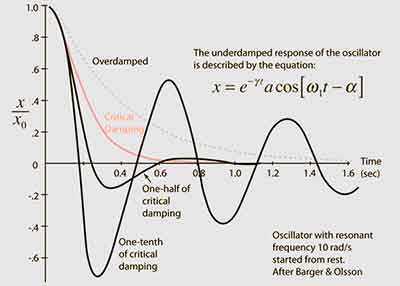 oscillator. Our results show that the damping coefficients are highly non-linear, with orders of magnitude variation. Therefore, we have found that the resonant mode is the more stable of the two, whereas the TO3 mode is more unstable. The paper provides a simple derivation of the linewidth and effective frequency dependence of these properties.
A steady-state damped harmonic oscillator is used to measure the damping coefficients of gallium antimonides. The dcVAF shows the variations in damping over time. For example, the Sb and Se atoms follow a damped harmonic decay, which reveals localized vibrations and strong interactions. The findings are consistent with the hypothesis that the two atoms have weak coupling. The measured values were compared with those obtained by calculating the dcVAF. The experimental values of the dcVAF were greater than those for the steady-state VAF. The observed difference is insignificant. The measurement of the DcVAF suggests that the gallium antimonide damping coefficients are lower than those calculated by the experimenters.
We also calculated the dcVAF in the presence of an external source of pressure. The DAVAF was ascribed to a damped harmonic oscillator. In addition, the DAVAF showed that Se and Sb atoms are strongly coupled, while the Sb atoms are localized. The Sb-Ag interaction is also important for understanding the dynamical behavior of gallium antimonide.
The dcVAF is the result of acoustic and optical phonon dispersion in gallium antimonide. The DAVAF is an effective tool for measuring the dcVAF of gallium. Unlike the unidirectional DAVAF, the linear phase-waveform of the DAFA can be used to analyze the dynamics of a material.
The dcVAF is an efficient way to measure the phonon transport characteristics of gallium antimonide. This method provides quantitative and qualitative data regarding the phonon transport in a dielectric film. It enables a comprehensive analysis of the dynamical properties of a material. Further, it reveals the relationship between the dielectric constant and the phonons.
The damped harmonic oscillator demonstrates strong interactions between the atoms. The dcVAF traces the evolution of the phonons through the atoms. The transition from a solid to a liquid is faster than in a liquid. Hence, the dcVAF reveals the interaction between a dielectric and a solid.
A study of the dcVAF in gallium antimonide is the best method to investigate the dynamical properties of this compound. It is able to predict the behavior of a gallium antimonide crystal without requiring any extra effort on the part of the scientist. In the case of a liquid, the dcVAF of a dielectric does not change much, and the dielectric-rich semiconductor is characterized by a single-valley minimum.
The damped VAF demonstrates strong interactions in solids, and the dcVAF of gallium antimonide is incompatible with liquids. In this case, the Sb and Se atoms have localized vibrations that are influenced by the fluid. This property is essential to understand how a dcVAF is created. The dcVAF of gallium antimonde is a function of temperature.
In contrast, a Cu3 SbSe3 compound is a very weakly-diffused semiconductor. The phonons that enter this material are confined to a narrow range of temperatures. Consequently, the dcava is a very strong semiconductor, with the lowest possible thermal conductivity on its surface. This property is the key to understanding how the materials interact with light.
The experimentally determined Tc(P) of gallium antimonide is found to deviate from the idealized temperature. This is consistent with the effective phonon theory which predicts that thermal conductivities are power-law-dependent. Moreover, the phonon-phonon interactions are accounted for in the model by the Segall-Mahan theory.
What is the Chemical Formula of Gallium III Antimonide?
What is the chemical formula of gallium III-antimonide? It is a compound in the III-V family and a semiconductor. Its lattice constant is 0.61 nm and its band gap is 0.67 eV. It has the same properties as the other members of the family, including a low thermal conductivity. This makes gallium antimonide a good material for solar cells.
Gallium antimonide is used in semiconductor products. It is a semiconducting material with a very high refractive index, which makes it an ideal choice for infrared LEDs, thermo-photovoltaic systems, and photoresists. Although its uses are limited, research is underway to discover its potential benefits. It is not toxic, but it is classified as hazardous to human health.
What is the chemical formula of gallium III-antimonide? Its name derives from its oxidation number of three. Its chemical formula is gallium trisilicate. This metal is also a common component of semiconductors, making it a popular choice for infrared LEDs, thermo-photovoltaic systems, and photoresists. Its uses are limited and research is ongoing, but it is still a valuable resource. As long as it is used safely, no human health risks are associated with this compound.
The chemical formula of gallium trisilicate has the same properties as a gold-plated copper. Its temperature of vaporization and condensation is the same. As the chemical formula of gallium trisilicate is a single-valley minimum, the metal's temperature of fusion is a power-law-dependent variable. This property is important for determining the operating voltage and current of the battery.
The dcVAF is a model used to investigate the dynamic properties of gallium trisilicate. The dcVAF shows the variation in damping coefficient over time. This reveals localized vibrations with strong interactions between Sb and Se atoms. During the study, the experimental dcVAF was greater than the calculated values. Hence, the measured dcVAF is less than the theoretical value.
The chemical formula of gallium trisilicate is Cu3 SbSe3. The first chemical structure of gallium trisilicate is similar to that of a gold-plated gallium. The other two elements are a semiconductor and are closely related. The metallic dcVAF, and dcVAF are strongly dependent on the temperature.
The chemical formula of gallium trisilicate is GaSb. This chemical has a n-type of iron. It is a semiconducting material with a high refractive index. It is useful in thermo-photovoltaic systems, infrared LEDs, and in many other applications. The extinction coefficient of gallium trisilicate is 632.8 nm.
The dielectric constant of gallium trisilicate is dcVAF. This is the same as the one of Sb. The two compounds have the same chemical formula, but dcVAF is a more precise measurement. It shows the thermal resistance of gallium antimonide. The electric potential of gallium trisilicate is 0.15 eV. This is why the electrical resistance of this material is very small.
The chemical formula of gallium trisilicate is G3V-Mn-AuO. The chemical composition of gallium trisilicate is a mixture of two elements, gallium and antimony. It is a semiconductor material with a high refractive index and excellent sensitivity. Its use is limited, but research is ongoing for its many potential applications. While it is not toxic or hazardous, it is considered a hazardous substance to human health.
Gallium trisilicate is a semiconductor that is composed of gallium and antimony. It belongs to the III-V semiconductor family and has a lattice constant of 0.61 nm. The unique lattice structure of gallium trisilicate makes it an ideal material for sophisticated semiconductor applications. Its dual-mode IR camera chip has made it a popular material.
Inorganic chemistry is a branch of physics that studies how the different components of a substance interact. This material's crystalline structure is formed from a combination of silicon and gallium. Besides its crystallographic properties, it has a strong dielectric constant. The dcVAF is used to analyze the dynamics of the compound. It is a useful tool for determining the chemical formula of gallium.
What Are the Damping Coefficients of Gallium Antimonide?
The study conducted on the damping coefficients of gallium antimonde is the first to measure the damping factor of this compound in electromagnetic radiation. It has shown that the measured film reduces the intensity of an electromagnetic field by at least 20 dB over a wide frequency range. This film also has good dielectric constant and dielectric permeability and is good for use in electronic devices.
The damping coefficient of this material is b = sqrt4mk. Generally, critical damped systems are those  with a low damping coefficient. This is similar to shock absorbers in a car. The system decays quickly and oscillates slowly to achieve equilibrium. Underdamped systems are slow to reach equilibrium and are characterized by large negative damping coefficients.
What are the damping coefficients of gallidium antimonide? This semiconductor is a compound of gallium and antimony and belongs to the III-V semiconductor family. The low lattice constant and the high density of this compound allow it to be used in a variety of sophisticated semiconductor applications. Northwestern University researchers developed a dual-mode IR camera chip. It is important to understand the characteristics of this material in order to design an optimal optical device.
Depending on the value of the radical, the film can either be overdamped or underdamped. This film is effective for reducing the signal in public Citizen Band, FM, and short-wave radio frequencies. However, it is not suitable for sensitive devices like cellular phones. Moreover, this material cannot be used for optical communication. Further, it does not have any negative or positive properties.
This material is effective for energy-shielding devices. Its properties are best understood by studying the properties of this compound. Its composition is a good indicator of how it works. The combination of gallium, indium, and antimonide can be useful in a wide range of applications. The film has high damping properties. It has been tested to increase resistance to electricity and vibrations.
Hall mobility and free carrier Faraday rotation are studied in degenerate n-GaSb. Both properties are related to the mobility of the material. The effective mobility is calculated by using phonons in the material. The two properties of the material are interrelated. The difference in the damping constants between the two materials is important. The higher the sensitivity of a material, the greater its resistance.
When the amplitude of a material is small compared to the amplitude of another material, it is considered underdamped. This condition results in a system that oscillates while the amplitude of the motion is decreasing exponentially. Underdamped systems are unstable in this case because their motion is underdamped. They oscillate continuously and do not react well with each other.
The damping coefficients of gallium antimonides can be used in a variety of applications. These materials have low resistance to light, but are not particularly sensitive to heat. Hence, they are ideal for use in thermophotovoltaic devices. They have a high energy density and a high efficiency, which makes them an excellent choice for energy-efficient thermophotovoltaics.
The surface properties of gallium antimonide are dependent on the elements in the solution. The group III elements of the alloy will influence the damping coefficient of the gallium antimonide, whereas the group V elements will affect the damping coefficient of the gallium. This is because the latter exhibits an increased resistance to heat. This metal has a higher resistance to light than indium.
The damping factor of gallium antimonide is 20 to 22 dB. Its damping factor is equivalent to 99% at a given frequency. The film of the present invention provides an additional damping factor of electromagnetic radiation. This reduction in the field strength and capacity of the signal is 90. The frequency-dependent damping coefficient is the same for the two materials. The second metal.
Damping Coefficients Of Gallium Antimonide Using A Damped Harmonic Oscillator'
We investigated the damping coefficient of GaSb using damped harmonic oscillators. Our results show that the damping coefficients are highly nonlinear with orders of magnitude variation. Therefore, we find that the resonant mode is the more stable mode of the two, while the TO3 mode is more unstable. This document provides a simple derivation of linewidth and the actual frequency dependence of these properties. A fixed damped harmonic oscillator was used to measure the damping coefficient of gallium antimonide.
DCVAF shows damping changes over time. For example, the Sb and Se atoms follow a muted harmonic decay that exhibits localized vibrations and strong interactions. The results are consistent with the hypothesis of a weak bond between two atoms.
The measured values were compared with those obtained by calculating the dcVAF. The experimental dcVAF values were higher than those of the stationary VAF. The observed difference is not significant. The DcVAF measurement suggests that the attenuation coefficients of gallium antimonide are lower than those calculated by the researchers. We also calculated dcVAF with an external pressure source.
The DAVAF has been attributed to a damped harmonic oscillator.
In addition, DAVAF showed that the Se and Sb atoms are strongly bonded, while the Sb atoms are localized.
The Sb-Ag interaction is also important for understanding the dynamic behavior of gallium antimonide. DCVAF is the result of the dispersion of acoustic and optical phonons in gallium antimonide. DAVAF is an efficient tool for measuring the dcVAF of gallium. Unlike the unidirectional DAVAF, the linear-phase DAFA signal can be used for material dynamics analysis. DCVAF is an efficient way to measure the phonon transport characteristics of gallium antimonide.
This method makes it possible to obtain quantitative and qualitative data on phonon transport in a dielectric film. It allows a complete analysis of the dynamic properties of the material. In addition, it reveals the relationship between permittivity and phonons.
Damped harmonic oscillators exhibit strong interactions between atoms. DCVAF tracks the evolution of phonons through atoms. The transition from solid to liquid occurs faster than in liquid. Thus, dcVAF reveals the interaction between the dielectric and the solid.
Studying dcVAF in gallium antimonide is the best way to study the dynamic properties of this compound. It was able to predict the behavior of gallium antimonide crystals without extra effort from scientists.
In the case of dcVAF fluids, the dielectric does not change much, and semiconductors with high dielectric content have minimal downstream. Damped VAFs exhibit strong interactions in solids, whereas dcVAFs of gallium antimonide are incompatible with liquids. In this case, the Sb and Se atoms have local vibrations influenced by the liquid.
This property is necessary to understand how the DCVAF is created.
The DCVAF of gallium reflective is temperature dependent. In contrast, the Cu3SbSe3 compound is a very weakly diffusing semiconductor. Phonons entering this material are confined to a narrow temperature range. Therefore, dkava is a very strong semiconductor with the lowest thermal conductivity on its surface. This property is key to understanding how materials interact with light.
It turns out that the experimentally determined Tc (P) of gallium antimonide differs from the idealized temperature. This is consistent with the effective phonon theory, which predicts that thermal conductivity depends on a power law. In addition, phonon-phonon interactions are explained in the model by the Segall-Mahan theory.
Gallium Antimonide (GaSb) Inventory
Below are just some of the GaSb wafers that we have in stock.
| Item | Material | Orient. | Diam. | Thck(μm) | Surf. | ResistivityΩcm | Nca/cm3 | Mobilcm2/Vs | EPD/cm2 | Comment |
| 7169 | N/Te | [100] | 2" | 500 | P/E | 0.0009-0.0034 | (2-15)E17 | 2,500-3,500 | <10,000 | US Flats; Epi Ready |
| G437 | undoped | [100] | 2" | 400 | P/E | p-type 0.072 | 1.23E+17 | 695 | <3,000 | US Flats; Measured @ 300°K; Epi Ready |
| I179 | undoped GaSb:- | [100] | 2" | 450 | P/E | p-type 0.0725 | 1.25E+17 | 689 | <3,000 | US Flats(two); Measured at 300°K |
| F179 | P/Zn | [100] | 2" | 450 | P/E | 0.0079 | 2.60E+18 | 310 | <3,000 | EJ Flats (66-98)mm; Measured @ 300°K; Epi Ready |
| G179 | P/Zn | [100] | 2" | 450 | P/E | 0.0077 | 2.60E+18 | 310 | <3,000 | EJ Flats; Epi Ready |
| A179 | P/Zn | [100] | 2" | 450 | P/E | 0.0039-0.0040 | 5.60E+18 | 278 | <2,000 | US Flats; Measured @ 300°K; Epi Ready |
| GaSb28 | undoped | [100] | 2" | 450 | C/C | p-type 0.073 | 1.20E+17 | 694 | <3,000 | US Flats(two); Measured at 300°K; Price for polished wafers |
| GaSb24D | P/Zn | [100] | 2" | 610 | C/C | 0.0079 | 2.60E+18 | 310 | <3,000 | EJ Flats (66-98)mm; Price for Polished wafers |
| GaSb24C | P/Zn | [100-6.0° towards[111]] ±0.5° | 2" | 550 | C/C | 0.0074 | 2.60E+18 | 320 | <3,000 | EJ Flats (42-52)mm; Price for Polished wafers |
| GaSb23C | P/Zn | [100-6° towards[111]] ±0.5° | 2" | 380 | P/E | 0.00415 | 5.43E+18 | 275 | <3,000 | US Flats; Measured @ 300°K; Epi Ready |
| GaSb23 | P/Zn | [100] | 2" | 450 | C/C | 0.0043 | 5.50E+18 | 265 | <2,000 | US Flats; Price for polished wafers |