⚡ In Stock Ready to Ship Silicon Wafers
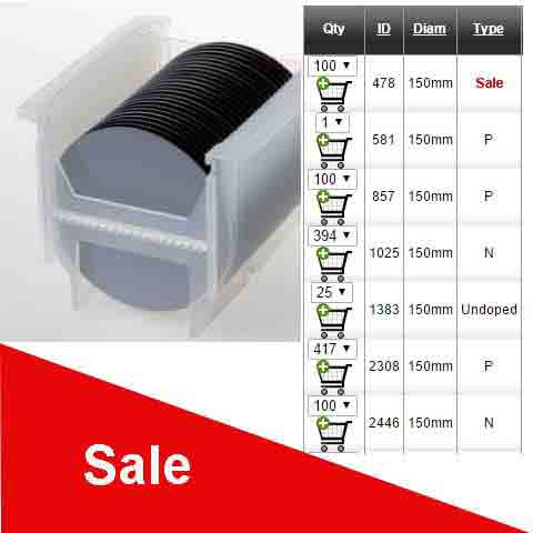
Below is just an example of what we have in stock. We also have P-Type, N-Type of all dopants and specs. Buy as few as one wafer!
100mm Undoped Silicon
(100) Orientation, >20,000 ohm-cm, SSP, 500µm Thickness.
We have 1,000 wafers of this spec available immediately.
Get Your Silicon Wafer Quote FAST! Or, Buy Online and Start Researching Today!
Why Buy From Us?
- No Minimums: Buy 1 wafer or 1,000.
- Global Sourcing: We source from top manufacturers like SUMCO to ensure semiconductor-grade quality.
- University Friendly: We accept Purchase Orders from all major universities.
Shop Silicon Wafers by Diameter
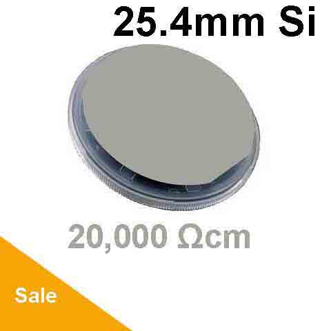
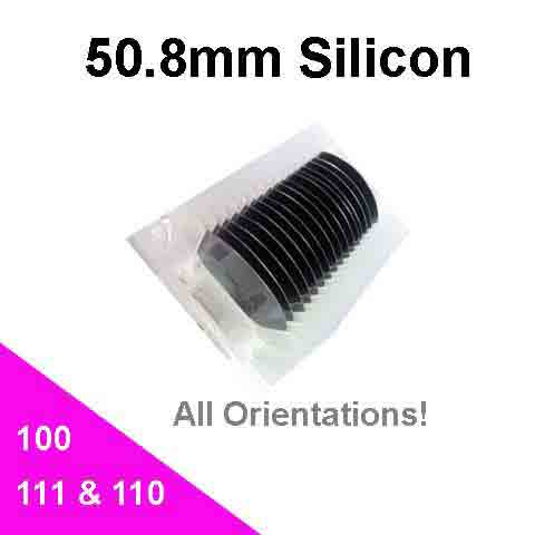
Browse our silicon wafer inventory by diameter to find available specifications, quantities, and pricing. UniversityWafer supplies silicon wafers from 1 inch (25.4mm) through 12 inch (300mm) for research, semiconductor processing, device fabrication, and production applications.
How to Choose the Right Silicon Wafer Specifications
Selecting the correct silicon wafer specifications depends on the fabrication process, electrical requirements, and intended application. Important parameters include wafer grade, crystal growth method, orientation, conductivity type, dopant, resistivity, thickness, and surface finish.
1. Silicon Wafer Grade
- Prime Grade: High-quality wafers manufactured to tight specifications for surface quality, thickness variation, bow, and warp. Prime silicon wafers are commonly selected for photolithography, semiconductor device fabrication, epitaxy, and other processes requiring a high-quality surface.
- Test Grade: A cost-effective choice for process development, equipment testing, thin-film deposition, oxidation, and laboratory experiments where prime-grade specifications may not be necessary.
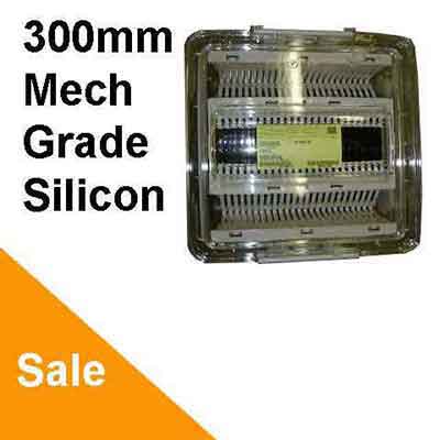
- Mechanical/Dummy Grade: Economical wafers intended primarily for equipment setup, handling practice, mechanical testing, furnace loading, dicing tests, and other non-device applications.
2. Crystal Growth Method: CZ vs. FZ Silicon
Czochralski (CZ) silicon is produced by pulling a single-crystal ingot from molten silicon contained in a quartz crucible. CZ silicon is widely available in many diameters, orientations, dopant types, and resistivity ranges and is commonly used throughout semiconductor research and manufacturing.
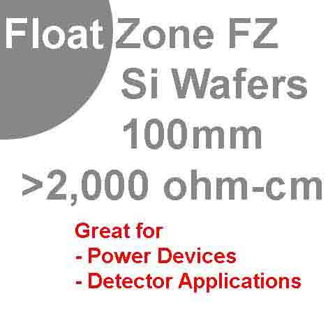
Float Zone (FZ) silicon is produced without a crucible, resulting in very low oxygen and impurity concentrations. FZ silicon wafers are often selected when high purity or high resistivity is required, including power electronics, RF devices, detectors, and specialized semiconductor research.
3. Silicon Wafer Orientation
Crystallographic orientation describes how the silicon crystal lattice is aligned relative to the wafer surface. Orientation can influence surface properties, anisotropic etching, oxidation behavior, epitaxial growth, and device fabrication.
- <100>: One of the most widely used silicon wafer orientations and common in CMOS, MOS devices, MEMS, and general semiconductor fabrication.
- <111>: Commonly used in specialized semiconductor processing, epitaxial growth, research, and applications where the crystallographic surface or etching behavior is important.
- <110>: Used in selected MEMS, microfabrication, surface-science, and semiconductor research applications.
4. Conductivity Type and Dopant
Silicon wafers are available as P-type, N-type, or high-purity/undoped material. Boron is a common P-type dopant, while phosphorus, arsenic, and antimony can be used for N-type silicon. The required conductivity type and dopant depend on the electrical characteristics of the device or experiment.
5. Resistivity
Silicon wafer resistivity is an important electrical specification and is typically expressed in ohm-centimeters (Ω·cm). Low-resistivity wafers are used when greater electrical conductivity is required, while high-resistivity silicon is commonly selected for RF, microwave, detector, photonics, and other applications where reduced substrate conductivity is beneficial.
6. Wafer Thickness
Silicon wafer thickness varies with diameter and application. Standard-thickness wafers are suitable for many semiconductor processes, while thin or ultra-thin wafers may be required for advanced packaging, sensors, MEMS, and specialized devices. Thick silicon substrates can also be supplied for mechanical stability, calibration, optical, and custom research applications.
7. Surface Finish: SSP vs. DSP
Single-side polished (SSP) silicon wafers have one polished device surface, while double-side polished (DSP) wafers provide polished surfaces on both sides. DSP wafers are often selected for wafer bonding, MEMS, optics, lithography, and processes where surface quality or flatness on both sides is important.
Common Silicon Wafer Applications
Silicon wafers are used as substrates across semiconductor research, microfabrication, electronics, optics, and materials science. The appropriate wafer specification depends on the processing steps and performance requirements of the application.
- Semiconductor Devices: Silicon substrates are used to fabricate integrated circuits, transistors, diodes, sensors, and other electronic devices.
- MEMS & Microfluidics: Silicon provides a well-characterized substrate for micromachining, anisotropic etching, microchannels, sensors, and microelectromechanical structures.
- Thin-Film Deposition: Silicon wafers provide a stable substrate for PVD, CVD, ALD, sputtering, evaporation, and experimental thin-film growth.
- Photonics & Infrared Research: Silicon substrates are used in silicon photonics and selected near- and mid-infrared optical applications.
- Nanotechnology & Materials Research: Silicon and silicon-on-oxide surfaces are commonly used for graphene, carbon nanotubes, 2D materials, nanostructures, and surface characterization.
- Equipment Testing & Calibration: Test and mechanical-grade wafers can be used for dicing, wafer handling, deposition system setup, furnace testing, and process calibration.
Need Help Selecting a Silicon Wafer?
UniversityWafer can help researchers and engineers identify silicon substrates based on diameter, orientation, dopant, conductivity type, resistivity, thickness, polish, and grade. Tell us the specifications required for your process and we can help locate an appropriate wafer from our inventory.
Get Your Silicon Wafer Quote FAST! Or, Buy Silicon Wafers Online and start researching today!
Related Silicon Wafer Resources
- What Is a Silicon Wafer? – Learn how silicon wafers are manufactured and why they are used as semiconductor substrates.
- Types of Silicon Wafers – Compare silicon wafer types, grades, orientations, dopants, and other specifications.
- Silicon Wafer Applications – Explore applications in semiconductors, MEMS, photonics, sensors, and materials research.
- Silicon Wafer Crystal Orientation – Understand (100), (110), and (111) silicon orientations and their uses.
- Silicon Wafer Resistivity – Learn how resistivity and doping affect silicon wafer electrical properties.
- How Silicon Wafers Become Computer Chips – See how silicon substrates are processed into semiconductor devices and integrated circuits.
- Silicon Wafer Flats and Notches – Learn how wafer flats and notches identify crystal orientation and other wafer characteristics.