
We are developing CMOS-based semiconductor devices and need 100 mm (100) prime-grade silicon wafers with a mirror-polished surface, controlled resistivity, and tight thickness tolerance for photolithography and MEMS fabrication. What specifications do you recommend?
Get Your Silicon Wafer Quote FAST!
UniversityWafer supplies high-quality silicon wafers and semiconductor substrates for universities, research laboratories, government facilities, and commercial manufacturers. Whether you need prime-grade, test-grade, DSP, SSP, SOI, or custom silicon wafers, our technical team can help you select the right substrate for your application.
From 25.4 mm to 300 mm diameters, we offer silicon wafers in multiple crystal orientations, resistivity ranges, thicknesses, surface finishes, and doping types for research, prototyping, and production.
Researcher Request
Popular Silicon Wafer Options
- Prime Grade Silicon Wafers
- Test Grade Silicon Wafers
- Single-Side Polished (SSP) Wafers
- Double-Side Polished (DSP) Wafers
- Silicon-on-Insulator (SOI) Wafers
- Thermal Oxide Silicon Wafers
- Heavily Doped Silicon Wafers
- Custom Silicon Substrates
Get Your Quote FAST! or Buy Online and start your research today.
Common Silicon Wafer Applications
- Semiconductor device fabrication
- Integrated circuits (ICs)
- Microprocessors and CPUs
- MEMS devices
- Power electronics
- Photonics and optoelectronics
- Sensors and biosensors
- Solar cell research
- University and government research
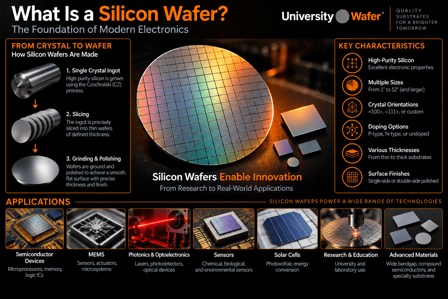
What Is a Silicon Wafer?
A silicon wafer is a thin, circular slice of high-purity single-crystal silicon used as the foundation for semiconductor devices, integrated circuits, MEMS, sensors, photonics, and other electronic technologies.
Silicon wafers provide a flat, highly controlled surface on which transistors, circuits, thin films, dielectric layers, sensors, and other micro- and nanoscale structures can be fabricated. Depending on the application, wafers may vary in diameter, thickness, crystal orientation, resistivity, dopant type, and surface finish.
Why Is Silicon Used for Semiconductor Wafers?
Silicon is widely used in semiconductor manufacturing because its electrical properties can be precisely controlled through doping, while its native oxide, silicon dioxide (SiO2), is extremely useful for insulation, passivation, gate dielectrics, and microfabrication.
Silicon is also mechanically stable, widely available, and supported by a mature manufacturing infrastructure, which is why it remains one of the most important substrate materials in modern electronics.
Key Silicon Wafer Specifications
The correct silicon wafer depends on the device, experiment, or fabrication process. Important specifications include:
- Diameter: Common wafer diameters include 25.4 mm, 50.8 mm, 76.2 mm, 100 mm, 150 mm, 200 mm, and 300 mm.
- Crystal Orientation: (100), (110), and (111) silicon orientations are commonly used depending on the fabrication process.
- Conductivity Type: Silicon wafers may be P-type, N-type, or undoped/high-resistivity.
- Dopant: Common dopants include boron for P-type silicon and phosphorus, arsenic, or antimony for N-type silicon.
- Resistivity: Resistivity helps determine the electrical behavior of the substrate and can range from highly conductive to high-resistivity material.
- Thickness: Wafer thickness varies by diameter and application, with standard, thin, ultra-thin, and thick silicon substrates available.
- Surface Finish: Wafers may be single-side polished (SSP) or double-side polished (DSP).
How Are Silicon Wafers Made?
Silicon wafer manufacturing begins with high-purity silicon and typically involves growing a single-crystal ingot, slicing the ingot into wafers, and then refining the wafer surface through grinding, lapping, etching, polishing, and cleaning.
- Crystal Growth: High-purity silicon is melted and formed into a single-crystal ingot, commonly using the Czochralski (CZ) process .
- Ingot Shaping: The silicon ingot is ground to the required diameter, and a flat or notch may be added for orientation identification.
- Slicing: The ingot is cut into thin circular wafers using precision wire-saw or other slicing processes.
- Edge Grinding: Wafer edges are shaped to reduce sharp edges and improve mechanical durability.
- Lapping and Etching: Surface damage and thickness variation introduced during slicing are reduced.
- Polishing: Chemical-mechanical polishing can produce the smooth, mirror-like surface required for many semiconductor processes.
- Cleaning: Final cleaning removes particles, metals, organics, and other contaminants before the wafer is used for device fabrication.
How Silicon Wafers Become Microchips
A polished silicon wafer is only the starting substrate. To create semiconductor devices, manufacturers repeatedly add, pattern, modify, and remove thin layers from the wafer surface.
- Oxidation and Deposition: Dielectric, semiconductor, and metal layers are formed on the wafer.
- Photolithography: Photolithography defines microscopic circuit patterns.
- Etching: Selected regions of material are removed to form device structures.
- Doping: Controlled impurities are introduced to create regions with desired electrical behavior.
- Metallization: Conductive interconnects are added to electrically connect transistors and other components.
- Testing and Dicing: Completed wafers are electrically tested and separated into individual silicon dies .
What Are Silicon Wafers Used For?
Silicon wafers are used in a wide range of research, manufacturing, and electronic applications.
- Integrated Circuits: CPUs, memory, logic devices, and microcontrollers.
- MEMS: Accelerometers, gyroscopes, pressure sensors, and microfluidic devices.
- Power Electronics: Diodes, MOSFETs, and other power semiconductor devices.
- Photonics: Optical components, waveguides, and silicon photonic devices.
- Sensors: Chemical, biological, pressure, temperature, and environmental sensors.
- Solar Research: Photovoltaic cells and related materials research.
- Thin-Film Research: PVD, CVD, ALD, sputtering, and experimental coatings.
- University Research: Semiconductor physics, nanotechnology, surface science, and materials characterization.
Silicon Wafer Sizes
Silicon wafers are produced in several standard diameters. Larger wafers can provide more usable device area per wafer, while smaller wafers remain widely used in research, prototyping, specialized equipment, and legacy fabrication processes.
- 25.4 mm (1 inch) silicon wafers
- 50.8 mm (2 inch) silicon wafers
- 76.2 mm (3 inch) silicon wafers
- 100 mm (4 inch) silicon wafers
- 150 mm (6 inch) silicon wafers
- 200 mm (8 inch) silicon wafers
- 300 mm (12 inch) silicon wafers
Choosing the Right Silicon Wafer
Selecting a silicon wafer requires matching the substrate specifications to the intended process. Researchers commonly consider diameter, thickness, orientation, conductivity type, dopant, resistivity, polish, growth method, and surface condition.
UniversityWafer supplies silicon wafers for semiconductor research, MEMS, photonics, thin-film deposition, microfabrication, equipment testing, and other scientific applications.