
Large Selection of Wafers from Al2O3 to Silicon to Zinc Oxide
What services can we provide? We have a large selection of bare silicon wafers that we can thin, dice, deposit thermal oxide, nitride, metals and more!
Contact UniversityWafer, Inc.
UniversityWafer, Inc. is located near our research clients at MIT, Harvard, Boston University, Northeastern University, Tuft and More Research Labs.
Immediate response. Fast delivery. Guaranteed quality.
What Do Scientist Ask UniversityWafer, Inc?
Below are just some samples of how we help researchers find the right substrate at a great price with fast delivery.
Silicon Wafer Specials
We help companies liquid their inventory and often have access to hard to find substrates at below market prices and in small quantities.
For example we have 6 inch and 8 inch inventory of SUMCO silicon wafers available for immediate delivery.
Quartz Wafer Carrier
We have a large selection of wafers packaged in both plastic and quartz wafer carriers.

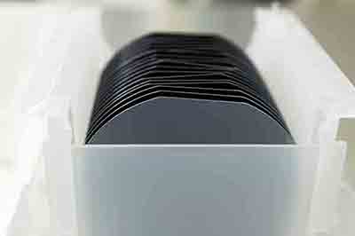
Silicon Wafers Plastic Cassette
Typical 100mm silicon wafers in their plastic case. The substrates are used to fabricate Integrated Circuits (IC) for the microelectronics industry.
Wafers for Terahertz Applications
Researcher Request:
Can you help me? Please quote HRFZ Silicon, Double side polished, more than 10k Ohm resistivity 2".
UniversityWafer, Inc. Reply
Our offer for the wafer for Terahertz applications
HRFZ Silicon 50.8mm Undoped (100) or (111) >10,000 ohm-cm >/=280um DSP PRIME FZ, Intrinsic, TTV<10um, Bow/Warp<30um, SEMI Flats.Qty. 10
$23.98usd/ea; 1~2 week delivery
Fused Silica Request
Researcher:
We have requirements for Fused Silica Windows Duly Polished: Fused Silica Wafer UV Grade (JGS1) Diameter = 50mm x Thick = 2.00mm Qty. 25 Pcs. Diameter = 50mm x Thick = 2.50mm Qty. 25 Pcs. Optical specifications: Surface 1: Surface Flatness: wave/4 (PV) @633 nm Surface irregularities < 5 nm Surface 2: Polished Scach-dig: 60/40 Kindly send us your lowest quote for the same. An early reply will be highly appreciated.
UniversityWafer, Inc. Quoted
The flatness you assigned here is Lambda/4, so it is 158nm, so irregularity must be even better than 158nm, are you mean the flatness cna be 5um, see our quotation below:
1) Fused Silica Window
Diam50x2.0mm thick, DSP
Flatness: 5um
S/D:60-40
Quantity: 25 Pieces
FOB Price: $15.90 each
Delivery Time: 2 Weeks
2) Fused Silica Window
Diam50x2.5mm thick, DSP
Flatness: 5um
S/D:60-40
Quantity: 25 Pieces
FOB Price: $16.90 each
GaN LEDs for chip assembly research
Good morning, I am interested in fabricating my own GaN LEDs for chip assembly research. In our facilities in the TU Ilmenau, we don´t have the technology to grow epi layer, so we are looking for a provider who can give us a substrate with the necessary layers on top, so that we just etch and contact it. Do you have any product that may suit our needs?
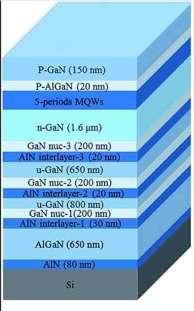
UniversityWafer, Inc. Quoted
The specific epi structure are ok,Pls see below for the offer 4'' GaN on Silicon <111> Blue LED Wafer
4'' Si-Based <111> LED GaN Epi structure Blue LED Wafer,Specific epi structure(susbstrate example),Qty: 10-25
Cutting Silicon Carbide (SiC) Filters
Researcher asked for the following quote:
I need 4x 4" diameter (SiC) wafers, polished to 38, 40, 46, and 53 um. Each wafer needs to be diced to 7x di, each di is 30 mm x 25 mm. Please let us know if this is possible and/or if we can discuss other options.
UniversityWafer, Inc. Quoted:
4" Diameter diced to 7pcs of 30mm x 25mm
Thickness: 38um, 40um, 46um, 53um, tolerance<5um

Researcher Replies and Then Order:
Yes, we would like to order these parts from you. A couple of things before we can place the order:
1. What is the lead time?
2. Can you send the di as they are ready?
3. Can you start with the 53 um wafer and send a di ASAP? We have some thermal experiments we need to perform with it.
4. Can you please provide a formal quote (PDF)? I have to submit this request through our university purchasing department.
5. I saw on the website there is a "research discount." Has this been applied? These will be used for nuclear research applications.
It will still be on the wafer dicing tape? I have done Si wafer dicing before (with thicker Si than this), and getting the die off without breaking them can be hard! I am worried about doing this myself, especially with such thin wafers.
Some dicing tape needs to be exposed to UV to remove the adhesive. We don't have this capability readily available in our lab. Can you please advise how we will be able to get the die off the tape? Will this be a trivial process? Are there special tools or chemicals we will need?
Is it possible to receive the die without the wafer tape attached?
UniversityWafer, Inc. Replied:
We need to attach the tape on wafers that are under 100um to avoid the breakage during the transportation. So we need customers to do the UV irradiation by themselves after they received the wafer. Please let me know if your customer really needs the die wafer without the tape attached, I will go talk to our manufacturer but there might be a price increase.
Customized Sapphire Wafers
Researchers Asked The Following:
Chris Do you accept customized thickness sapphire wafer order? We want to order sapphire wafer with size of 100mm, thickness of 800um. These wafer will be used as backing wafer for GaAs grinding/polish process. Qty is 10 pieces. Rest of the spec same as you standard sapphire product: 2562. C-M plane 0.2°, Double Side Polished, Micro-roughness: Ra<0.35nm, Primary flat length: 32.5±2.5mm. Warp<21um, TTV<16um.
UniversityWafer, Inc. Quoted and Researcher Purchased:
100mm, thickness of 800um. used as backing wafer for GaAs grinding/polish process. Qty is 10 pieces. Rest of the spec same as you standard product: 2562. C-M plane 0.2°, Double Side Polished, Micro-roughness: Ra<0.35nm, Primary flat length: 32.5±2.5mm. Warp<21um, TTV<16um. (254745)
Thermal Oxide Coated Silicon Wafers for Biomedical Research
Scientists have used the following thermal oxide item for Biomedical applications
Si Item #1583
100mm P/B <100> 0.001-0.005 ohm-cm 500um SSP Prime w/ 300nm Wet Thermal Oxide with Thickness Tolerance +/- 7%
Single Crystal Quartz for Diffraction Experiments
Researcher purchased the following quartz substrate.
"We are using the quartz plates for manufacturing samples for laser experiments. When hitting the sample with the laser it will be damaged so that we need to purchase quartz crystals over the over again until the project is completed."
Seedless Quartz Item #3064
50.8mm Z-cut 50um DSP Seedless
Typical Sapphire Single Wafer Carrier
Below is a typical single wafer carrier. We have all diameters.

Sorting Polished Silicon Wafers
We sell as few as one wafer!

Silicon Pellets
Researcers use Silicon Pellets as a source material for chemical vapor deposition and physical vapor deposition. These are high-performance, low-cost, high-quality silicon pellets.
Semiconductor “Chips are the New Oil”
So, say those in power and Lesley Stahl on 60 Minutes, who understand just how important the semiconductor industry is to the US and global economy.
The US semiconductor industry was subsidized once. In the 80s, The Reagan Administration was engaged in staving off the loss of the US semiconductor industry to the Japanese by providing billions in grants and subsidies to US based semiconductor companies. Unfortunately, during the first Bush president, policy shied away from Reagan’s proactive stance. Bush’s economic adviser publicly showed his disdain of semiconductor industry. “Potato chips, computer chips, what’s the difference?” This laissez faire policy turned a thriving US semiconductor industry to what it is today. Anemic. The Asian countries subsidized their burgeoning semiconductor industry into the behemoths they are today.
Why can’t current industry players build new plants? The cost of constructing a new semiconductor plant is in the billions and takes years to approve permitting and construction. Thus, without US government intervention through subsidies and zoning laws, few if any companies will take on such a challenge. Intel is trying in Arizona. But the severe drought, and if it continues, may dissuade Intel from proceeding. You need a lot of water to make a microchip. In fact it takes 10 gallons to make one microchip. This is a problem when you’re fabricating tens of millions of microchips! And the waste water contains toxic acids and metals.
Unlike an automobile that takes Ford less than one day to make from components.
Semiconductor microchips take around 85 days morph from silicon wafer that range from 25.4mm to 450mm into microchip. Plants or Fabs are expensive to make and only the most expensive equipment will do. But just buying equipment does not a fab make. Workers, including technicians, salesman, managers etc. have to work together as a team. This is more difficult than it sounds. Think of a baseball team. The pro teams have farm teams that feed talent to the big leagues. A new semiconductor plant’s farm teams are in the PHD programs of universities. There students, learn how to work with others while sporting bunny suits. Even so, how many pro teams are actually elite? Not many! Talented personal that can work efficiently as a team are difficult and expensive to put together. Not to mention many PHDs are foreigners who must rely on visas to work and study here in the states. They suffered under the previous administrations immigration policies.
But there is hope!
Government policy wise there is good news is on the horizon. Currently U.S. lawmakers are changing course. In June the Senate drafted a bill, titled U.S. Innovation and Competition Act. Bluntly the US will be subsidizing semiconductor manufacturing again.
“This is infrastructure,” exclaimed President Biden while holding a 300mm polished silicon wafer, this past spring, at the White House. For Biden, selling high-tech from polarizing Silicon Valley as infrastructure is a good way to get even the most reluctant luddite or Republican to vote for the bill. Perhaps soon the US will lead the world in Semiconductor manufacturing again!
But how long will it take to regain the lead? Well, it takes about 90 days to fabricate approximately 66 layers of chemicals, metals etc. onto a 300mm silicon wafer to create microchip found in computers electronic components autos to toy widgets.
It should start now. The pandemic has proven the just in time inventory is a national security issue today as oil was in the recent past. In the early 1990s, around 37% of chips were
made in US factories, that number collapsed to just 12% today. Asia has the rest.
There is plenty of room for improvement!
Silicon Wafer Shortage
Unlike many other firsm, UniversityWafer, Inc. has a large selection of substates for sale online. Why wait weeks for your current supplier when we have the wafers in stock!
11 Elkins Street
Unit 330
South Boston, MA 02127
UniversityWafer, Inc.
3651 FAU Boulevard Suite 400 Boca Raton, FL, 33431
![]()
![]()
![]()
![]()