
Our project is looking for sapphire-on-silicon (or silicon-on-sapphire) wafers used for 2D TMD material growth. We prefer a thin layer of sapphire grown on a silicon wafer, but it works with silicon on sapphire too. Can you provide a quote for the silicon-on-sapphire wafers with silicon film thickness of 1.5um, 0.6um and 100nm? Each type with a quantity of 3?
SoS Substrates for 2D Material Research
A PhD candidate requested a quote for the following:
Reference #270456 for specs and pricing.
Get Your Quote FAST! Or, Buy Online and Start Researching Today!
Pre-cut 4'' Silicon-on-Sapphire (SOS) Wafer
We can pre-cut SoS wafers into diced pieces.
Sapphire thickness 460+/-25um,we have 400nm SOS based on 460um DSP R-sapphire,if need SSP SOS,we have it with >/=600nm Si on 460+/-25um SSP Sapphire.

Wafers for Metasurfaces Research
600nm thick Silicon deposited on on sapphire wafers have been used from research clients for their academic research metasurfaces.
Our Research Client States:
We will use e-beam lithography to fabricate designed silicon
nanostructures on the sapphire wafer, which is called as
metasurface.
Metasurfaces can be used to manipulate the wavefront,
propagation direction, or focusing of light.
Silicon-on-Sapphire Refractive Index
A researcher asks:
I am interested in Si on Sapphire Wafer(SOS) for some experiments. And I have a few questions. 1. I want to know the refractive index of Si for the light with wavelength of 850nm. Is it okay to think that your Si on wafer has the same refractive index as bulk crystalline silicon whose refractive index for 850nm is n=3.673 and k=0.005? If it is not correct, would it be possible to know the refractive index? 2. Does your company have an agency in Japan which I can buy through? I look forward to hearing from you soon.
UniversityWafer replied:
The refractive index shoud be the same, because the si film on sapphire was the same single crystal silicon <100>.
How to Commercialize Silicon-on-Sapphire (SoS) Wafers
Video: Silicon on Sapphier Applications
Diced Silicon-on-Sapphire Wafers
A PhD student requeted diced SoS wafers from our inventory.
What I need would be a diced wafer (can be either in waffle pack or still in the tape) and the Dies will need to be wirebondable and die bondable. I am also needing the substrate and lead frames. The dies does not need to be functional, I just want to test out some wirebond machines output using these Units. If you need we can do an online meeting.
We can do cutting service for you,like as the attached diced 4'' SOS Wafer.

Silicon-on-Sapphire Sapphire to Fabricate Metasurface
A PhD student requested the following qutoe:
We are looking for Si (~600-700 nm thick) on Sapphire substrates. If you could precut the substrate into 1cmx1cm chips, it would be great.
We are using this to fabricate metasurface with subwavelength-thick phase gradient to generate high Q-factor resonances, by e-beam lithography. The incident laser will be around 1500 nm. PFA for the paper for the reference.
Silicon EPI Layer:
Silicon Orientation: (100)
Type, Dopant: Intrinsic type, undoped
Silicon Thickness: 0.6 um
Resistivity: > 100 ohm.cm
Micro-particle density ( for particles > 2 um) < 2/cm^2
Sapphire Wafer:
R plane -- (1-102) with single flat
Purity: 99.996%
Wafer size: 100 mm dia x 0.46 mm thickness
Flat : One flat 32.5mm +/-2.5mm, at 45+/- 1 deg CCW from <C> on <R>
Front surface: Epi-polished (Ra < = 0.3 nm)
Back surface: Optical grade polish
TTV < 15 um, Bow < 20 um, Warp < 20 um, Flatness (TIR) < 12 um, with Laser Mark on wafer back-side, just below the Flat
Could you give us a quote on 1, 5 and 10 chips? Then we could decide how many to purchase.
RFQ #258665 for specs and pricing.
What Silicon-on-Sapphire Used For Optical Metasurface Application?
A research scientist requested a quote for the following:
We are looking for crystalline Silicon on sapphire wafers for an optical metasurface application. We ideally seek a silicon layer thickness in the range of 500-600 nm, and it is desirable that the materials exhibit low absorption loss.
UniversityWafer, Inc. Quoted:
Crystalline Silicon on 4" Sapphire Wafers for an optical metasurface application. silicon layer thickness 500-600 nm.
For optical metasurface applications, especially when using crystalline silicon on sapphire (SOS) wafers, several key factors need to be considered to ensure optimal performance, particularly concerning the layer thickness and absorption losses.
Key Specifications:
- Silicon Layer Thickness: 500-600 nm
- Substrate: Sapphire
- Low Absorption Loss: Essential for optical applications to ensure high efficiency.
Supplier Recommendations:
-
University Wafer:
- We offer a variety of crystalline silicon on sapphire wafers.
- We provide customizable options for layer thickness and can cater to specific research requirements.
Reference #312424 for specs and pricing.
What Is A Optical Metasurface?
An optical metasurface is a two-dimensional, ultra-thin structure composed of subwavelength-sized elements known as meta-atoms. These meta-atoms can be engineered to manipulate light in ways that conventional optical materials cannot. Here are some key aspects of optical metasurfaces:
-
Manipulation of Light: Optical metasurfaces can control various properties of light, including its phase, amplitude, polarization, and direction. This allows for the creation of devices with unique functionalities, such as flat lenses (metalenses), holograms, and beam shapers.
-
Subwavelength Features: The meta-atoms are typically smaller than the wavelength of light they interact with. This subwavelength scale enables precise control over the interaction between light and the material.
-
Design and Fabrication: These surfaces are designed using advanced computational methods to achieve the desired optical properties. They are fabricated using techniques like electron-beam lithography or nanoimprint lithography, which allow for the precise patterning of materials at the nanoscale.
-
Applications: Optical metasurfaces have a wide range of applications, including in imaging systems, augmented reality devices, optical communications, and sensors. They can be used to create compact and lightweight optical components, potentially replacing bulkier traditional optics.
-
Material Choices: Metasurfaces can be made from a variety of materials, including metals, dielectrics, and semiconductors. The choice of material depends on the specific application and the desired interaction with light.
Overall, optical metasurfaces represent a significant advancement in photonics and optical engineering, enabling new capabilities and more compact, efficient optical devices.
Related UniversityWafer resources: Sapphire Wafers (Al₂O₃), Silicon Materials, Silicon-on-Insulator (SOI), 2D Materials Research, E-Beam Lithography, Photonic Crystals, MEMS Materials, Contact UniversityWafer.
What are Silicon-on-Sapphire Substrate?
Silicon on sapphire (SOS) substrates are thin films of silicon that are grown on sapphire wafers. Sapphire is a type of crystalline aluminum oxide that is known for its high strength and thermal stability, making it an ideal substrate material for microelectronic devices. The thin film of silicon is then used as a substrate for the production of microelectronic devices using various fabrication processes such as photolithography, etching, and deposition.
SOS substrates are used in a variety of applications that require high-quality, high-performance microelectronic devices. Some of the key advantages of SOS substrates include:
-
High thermal stability: The sapphire substrate provides excellent thermal stability, making SOS substrates suitable for use in high-temperature environments.
-
High electrical insulation: Sapphire has a high electrical breakdown field, making SOS substrates suitable for use in high-voltage applications.
-
High strength: Sapphire is a very hard and strong material, making SOS substrates resistant to mechanical damage and wear.
-
High radiation resistance: Sapphire is also highly resistant to radiation, making SOS substrates suitable for use in radiation-sensitive applications such as in space or in nuclear power plants.
Overall, the main advantage of SOS substrates is their ability to provide a stable, high-quality substrate for the production of microelectronic devices, particularly in environments that require high thermal stability, high electrical insulation, high strength, and high radiation resistance.
Why Use Silicon-on-Sapphire (SoS) Wafers?
Most Silicon-to-Sapphire (SoS) devices are fabricated by a 1985 patented process by Armen Sahagen. Devices include pressure transmitters, pressure transmitters, temperature sensors and membranes. SoS technology is great for sensor technology resulting in long-term stability. This is a major advantage over non-SoS-bound silicon sensors. New dielectric sensors made of silicon-on-sapphire (SoS) are attracting great interest and are being integrated into optical devices used in smartphones and tablets.
UniversityWafer, Inc. and our partners Silicon-on-Sapphire Wafers (SoS), have EPI layers to control the thickness for extremely tight Total Thickness Variation (TTV) and flatness specs on Kyropoulos grown sapphires.
Silicon-on-Sapphire (SoS) wafers are compatible with standard semiconductor processing equipment.
Companies that Use Silicon Sapphire (SOS) Wafers
The subtrates benefits have been attacted companies, including Apple, Google, Microsoft, Samsung and Samsung Electronics.
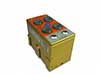
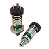
Typical Silicon-on-Sapphire (SoS) Packaging for One Wafer

Silicon on Sapphire (SoS) Applications
The advantage of sapphire is that it is an excellent electrical insulator, preventing stray currents caused by radiation from spreading to nearby circuit elements. When silicon is grown on sapphire, the resulting SoS substrate are used to fabricate IC devices. Often SoS wafers are used instead of Silicon-on-Insulator when a device requires less parasitic device capacitance, and increased device efficiency under high-temperatures.
But the problems with epitaxial silicon growth on sapphire wafers are lattice mismatch, discordant thermal expansion coefficients and limited silicon size. The Si-sapphire interface is home to a thick, defective region. After solid-phase epitaxial growth (SPER), Si is injected to reduce the density of defects. Two-phase epitaxial regrowth (SPER), film thinning and two-step epitaxy all provide sophisticated methods for material improvement. The bonding and Smartcut are the best methods to produce the highest quality SOS wafers.
Analog-to-Digital Converters

Monolithic Digital Isolation Buffers
SOS-CMOS image sensor arrays
Patch-Clamp Amplifiers

Energy Harvesting Devices
Three-Dimensional (3D) Integration with no Galvanic Connections
Charge Pumps
Temperature Sensors
Silicon-on-Sapphire R-Plane Al2O3
The 60° angle known as the R plane reveals the oxygen atoms in the crystal, and the distance between them is identical to that in the silicon crystal when silicon is deposited on the surface of the sapphire wafer. SOS is involved in epitaxial growth of silicon on a sapphire substrate (Al2O3).
Applications of this process are found in manufactured MOs and devices that include silicon cleaning processes to mitigate crystal defects resulting from mismatches in the sapphire silicon lattice.
Below are just some of the Silicon-on-Sapphire Wafers that we have in stock!
| Size (") | Orientation | Thick(μm) | Pol | Qty | Grade | Si Film Thickness |
| 4 | R-plane+/-0.5° | 460+/-20 | SSP | 50 | Prime | 0.6um <100> Si |
| 4 | R-plane+/-0.5° | 460+/-20 | SSP | 2 | Prime | 0.6um <100> Si |
| 4 | R-plane+/-0.5° | 460+/-20 | DSP | 10 | Prime | 0.6um <100> Si |
| 4 | R-plane+/-0.5° | 530+/-20 | DSP | 4 | Prime | 100+/-10nm <100> Si |
| 4 | R-plane+/-0.2° | 530+/-20 | DSP | 4 | Prime | 230+/-10nm <100> Si |
| 4 | R-plane+/-0.2° | 530+/-20 | DSP | 4 | Prime | 1.5+/-0.15um <100> Si |
| 4 | R-plane+/-0.5° | 460+/-20 | SSP | 4 | Dummy | |
| 6 | R-plane+/-1° | 600+/-20 | SSP | 1 | ||
| 8 | R-plane+/-2° | 725+/-20 | SSP | 1 |
SoS wafers to Fabricate Dielectric Resonantors
A new dielectric sensor fabricated from Silicon-on-Silicon (SOS) is attracting great interest as an integrated optical device for use in smartphones and tablets.
Scientists are reseaching fabricating dielectric resonator capable of maximising the maximum power of the sensor and its optical properties in the form of an optical sensor using SoS.
What are Silicon-on-Sapphire Wafers Used For?
Researchers have used the following SoS wafer specs to fabricate photonic crystal structures using e-beam lithography.
1 item of Pre-cut 4" Silicon on Sapphire Wafer, DSP, 100nm of Si film layer.
Qty. one wafer
dicing into 10x10mm chips.
Silicon orientation is 100
Silicon-on-Sapphire (SoS) for Photonic Waveguides
A larger university researcher was interested in SoS wafers for their work on Photonic waveguides. The researcher asked:
I have some questions that I would like to get answered first: What is the resistivity of the Si layer? Is it possible to get Si resistivities in the order of >3000 Ohm.cm? What is the Si crystal orientation in relation to primary flat for the R plane sapphire wafers? What is the purity of the EPI grown Si crystal? What can we expect in terms of monocrystallinity of the Si layer? What is the minimum qty for purchase? What is the lead time? If you have any other information for me I would love to hear it. Looking forward to your response!
UniversityWafer, Inc. Quoted our Thin SoS:
Pls see below for the offer on thin SOS Wafer
Dia.(inch) Orientation Si film thick. Surface Resistivity Substrate Thick
4'' R+/-0.5deg 200+/-10nm P/P $Conact us>100 Ohm.cm 460+/-20um
4'' R+/-0.5deg 300+/-10nm P/P $Conact us>100 Ohm.cm 460+/-20um
What Silicon-on-Sapphire (SoS) Wafers are Used for Dichroism Information From Sapphire Cyrstal Orientation?
Scientist requested:
Good morning, I hope you are doing well. I was wondering if you have single-crystalline silicon thin film (130 nm) on Sapphire 100mm substrate?
UniversityWafer, Inc. Replied:
Yes. 130nm silicon on sapphire.
We are very interested to have more information about the loss and refractive index ( n,k values) of different types of Sapphire (KR and CZ), the dichroism information from the crystal orientation, and the loss and refractive index (n,k values) of your available silicon layers ( e.g. a-silicon, H:Si, EPI silicon). Our wavelength range of interest is 700 to 800 nm.
I am looking forward to receiving the information regarding the n,k values of the silicon thin films and the sapphire.
Reference #260682 for specs and pricing!
What You Need to Know About Silicon on Sapphire
If you've never heard of silicon on sapphire, you're missing out. This semiconductor material is a crystal match for CMOS, but it also excels in linearity. Its linearity makes it a good choice for RF switches, a market that is hot right now. Read on to learn about this new material and what it has to offer. Listed below are a few applications and costs.
Heteroepitaxial growth
The process of heteroepitaxial growth of silicon on sapphire (SoS) involves depositing a thin layer of silicon on the sapphire substrate. Sapphire is an insulating material that makes the growth of silicon on sapphire advantageous for electronic applications. Its advantages include reduced parasitic capacitance, improved linearity, and lower power consumption compared to bulk silicon.
Heteroepitaxial growth of silicon is especially effective on sapphire substrates, as sapphire is a non-polar material. This non-polarity greatly influences the performance of the a-plane semiconductor. Furthermore, a-flat sapphire is easier to polish than c-plane sapphire, which is used for semiconductor devices. It is therefore the preferred substrate for heteroepitaxial silicon growth.
The RBS measurements are complementary to TEM studies of interfaces between the substrate and the deposit. They are useful for identifying regions of differing degrees of disturbance over the substrate surface. They also allow researchers to determine how substrate-deposit orientations influence heteroepitaxial silicon. This asymmetry is a potential source of instability, but it can be resolved by computer simulations. Heteroepitaxial growth of silicon on sapphire could ultimately be a successful technology for semiconductor devices.
The Rz of the surface of a single crystal of sapphire was measured at about ten Angstroms. The surface roughness was processed in the order of atoms and molecules. In addition, the electronic microscopic observations of the polished surfaces using conventional diamond grains and colloidal silica were similar. Hence, the technique is considered a promising option for high-quality sensor interfaces.
A similar process, known as tunnel epitaxy, allows the formation of single-crystal silicon. The silicon is deposited through seed windows on an oxidized Silicon substrate. Growth begins through the seed window and proceeds on the surface oxide. Unlike tunnel epitaxy, the CELO variant is much lower-temperature compared to ZMR and makes heteroepitaxy of III-V semiconductors possible. ELO6 is also considered a possible candidate for 3D integration.
Residual Dislocations
A new study has characterized the atomic structure of residual dislocations in sapphire. This new model, called basal twinning, provides an explanation for why some dislocations remain unaltered while others disappear. This study was able to demonstrate the importance of the dislocation cores in plasticity in crystalline solids. A detailed atomic model of the dislocation core was obtained, revealing a twinning partial, basal twinning, in intermediate temperatures.
Moreover, the spatial cathodoluminescence mapping revealed that these defects may be caused by different growth mechanisms. The spatial CL mapping supported two possible dislocation growth mechanisms. In window regions, the dislocations grow upward toward the top facets. Therefore, these defects are likely to occur during refractory annealing. This is one of the possible explanations for the high number of residual dislocations in sapphire.
Residual dislocations on sapphyre may be found in other nonmetallic solids. A high proportion of residual dislocations may be bending 90 degrees, and a frustum patterning substrate can be used to grow high-quality a-Ga2O3 epilayers. These studies demonstrate the power of this new growth method. A conical frustum patterned sapphire substrate is a potential choice for high-quality a-Ga2O3 epilayers.
The residual dislocations observed in the two-step-grown GaN on sapphire substrates show a high degree of influence on the growth of GaN on sapphire. These residual dislocations accumulate in the MOCVD reactor and influence the initial nucleation process of the GaN layer. To overcome this issue, a novel growth strategy is proposed. TMGa and NH are added to the high-temperature surface treatment process.
Silicon on Sapphire Applications
High-purity sapphire crystals are commonly used in SOS technology. The epitaxial growth of silicon on sapphire substrates mitigates the crystal defects by decomposing silane gas on the crystal surface. Silicon deposited on sapphire is a good electrical insulator and prevents stray currents from spreading through the material. Initially, the process was challenging because of crystal lattice disparities.
Despite the cost of sapphire substrates, high-quality epitaxial layers can be fabricated. Silicon on sapphire circuits can provide advantages like low parasitic capacitance, increased speed, improved linearity, and less power consumption. In addition, these devices offer higher levels of isolation than bulk silicon. This technology has many uses and is quickly becoming a major part of silicon microelectronics.
In the mid 1960s, research began on a new semiconductor that would be compatible with CMOS. This material was made of silicon and grew in specific locations. These sites corresponded to the R-plane of the sapphire crystal. This technology was eventually developed and commercially available. With its many benefits, silicon on sapphire is now used in a wide variety of products. One example of an application for silicon on sapphire is the development of RF switches.
Silicon on sapphire (SOS) devices are able to measure pressure at extremely high pressures. They have excellent long-term stability. The technology also has an advantage over non-SOS-bonded silicon sensors. Because the silicon Wheatstone bridge is formed during the manufacturing stage, this material has no residual stresses, non-repeatability errors, or bonding agents that can increase instability over time. This makes it possible to build high-quality silicon on sapphire devices for demanding applications.
The patented process used for Silicon on Sapphire fabrication enables the fabrication of a wide range of photonic devices. These devices are used for temperature sensors, pressure transmitters, and membranes. The technology has become so advanced that the semiconductor industry has rushed to develop new products based on the new material. In recent years, researchers have fabricated various photonic crystal structures using silicon on sapphire wafers.
What Do Silicon-on-Sapphires Wafers Cost?
Silicon-on-Sapphire is a hetero-epitaxial process for integrated circuit manufacturing. This semiconductor material, typically 0.6 micrometres thick, is part of the Silicon on Insulator (SOI) family. It is primarily used in military and aerospace applications. The process is expensive to produce, and is subject to stringent export regulations. To export the material to an overseas customer, an end-user certificate must be filed with the U.S. Department of Commerce. This is required for all sales, including international exports.
The global sapphire substrate market is highly fragmented and competitive. According to Transparency Market Research, there is a comparatively high level of competition among manufacturers. Meanwhile, the price of sapphire is expected to increase in the coming years. However, demand for sapphire technology is expected to remain strong for the foreseeable future. Thus, manufacturers should be prepared to increase their prices to meet rising demand. While the global sapphire substrate market is expected to grow at a healthy pace over the next few years, the industry will continue to face challenges.
The global sapphire substrate market is split into four main geographic regions: North America, Europe, and Rest of the World. In terms of revenue, Asia Pacific dominates the global sapphire substrate market, followed by Europe. However, the global market for sapphire substrates is expected to expand at a CAGR of 5.2%. Further, the global market for sapphire substrates is expected to rise significantly through the forecast period.
As the second most abundant element on earth, silicon is an essential component for computer chips. Because of this, it requires a complex process to produce silicon wafers. The process begins with a special sand called silica sand, which contains high concentrations of quartz and silicon dioxide. These two compounds are combined to produce the semiconductor. The resulting material has many properties and can be used in various applications.
To improve the quality of silicon on sapphire, HF and SC1 can be applied over the substrate. These solutions are effective in removing surface roughness on sapphire substrates. Silicon oxide also promotes the conductivity of dielectric layers deposited on sapphire. For example, silicon dioxide is an excellent conductor of electricity. Therefore, silicon on sapphire is a superior material for electronic devices.