
Prime Grade Silicon Wafers
UniversityWafer specializes in supplying Prime Grade (Device-Quality) silicon wafers to university laboratories, R&D centers, and semiconductor foundries. These wafers meet strict SEMI Standards for flatness and particle counts.
Our inventory includes a comprehensive range of specifications ideal for Epitaxial growth, Photolithography, and MEMS:
- Thickness: From 5µm ultra-thin silicon up to 10mm thick pucks.
- Surface Finish: Single Side Polished (SSP) or Double Side Polished (DSP) with CMP haze-free finish.
- Resistivity: Full range from highly doped (low resistivity) to intrinsic (high resistivity).
- Orientations: <100>, <111>, <110> available.
Looking for budget-friendly options?
We also stock a massive selection of Test Grade Silicon Wafers, perfect for process testing, particle monitors, and equipment calibration.
Get Your Silicon Wafer Quote FAST! Or, Buy Online and Start Researching Today!
Understanding Silicon Wafer Grades
Selecting the correct substrate grade is critical for experimental success. We offer the following tiers:
| Grade | Primary Use Case | Key Features |
|---|---|---|
| Prime Grade | IC Production, Photolithography, SOI Bonding | TTV < 1µm, Low Particles, Device Quality |
| Test Grade | Equipment Testing, Thin Films, Sputtering | Looser tolerances than Prime, Cost-effective |
| Mechanical Grade | Spin Coating, Dummy Wafers | Lowest cost, looser flatness specs |
Why Choose Prime Grade Silicon?
Prime grade silicon wafers (also known as Device Quality) are the highest quality substrates available. They are required for:
- Integrated Circuit (IC) Fabrication: The surface must be defect-free to ensure transistor reliability.
- Advanced Photolithography: Tight Total Thickness Variation (TTV) is crucial for focusing optics at sub-micron levels.
- Oxidation and Deposition: Ideal for high-quality Thermal Oxide growth or Nitride deposition.
- Particle Sensitivity: Prime grade wafers have the lowest particle counts, preventing shorts and open circuits.
Popular Research Substrates
For researchers who need high quality without the full production price tag, Test Grade wafers are often the standard choice.
Best Selling Research Item:
Item #452 - 100mm P(100) 0-100 ohm-cm SSP 500µm
Available for purchase in single wafer quantities.
Technical Specifications & Availability
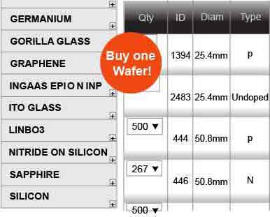
Standard Diameters In Stock:
- 25.4mm (1 inch)
- 50.8mm (2 inch)
- 76.2mm (3 inch)
- 100mm (4 inch)
- 125mm (5 inch)
- 150mm (6 inch)
- 200mm (8 inch)
- 300mm (12 inch)
Dopant Types & Growth Methods:
- P-Type (Boron/Gallium): Generally Czochralski (CZ) grown. Standard for most logic devices.
- N-Type (Phosphorous/Arsenic/Antimony): CZ grown. Used in electrons-as-carrier applications.
- Intrinsic / Undoped: Produced via Float Zone (FZ) method. These wafers offer high resistivity and high purity for detectors and power devices.
Researcher FAQ: Prime Grade vs. SEMI Standards
- Q: What is the difference between SEMI Prime and Prime Grade?
- A: There is no difference. "Prime" is simply the shorthand for "SEMI Prime." SEMI (Semiconductor Equipment and Materials International) is the governing body that sets the specifications. If a wafer is sold as "Prime," it must meet these rigorous SEMI standards for flatness and cleanliness.
- Q: What is an Empak Cassette (cst)?
- A: An "Empak cst" refers to the wafer carrier box. Empak is a leading manufacturer of these polypropylene carriers, which are the industry standard for safely storing and transporting silicon wafers to prevent particle contamination.