
When were 150mm Silicon Wafers Introduced?
Introduced in 1983, 150mm (5.9 inch, usually referred to as "6 inch") wafers can use the CZ or FZ method for ingot growth.
Get Your 150mm Silicon Quote FAST! Or, Buy Online
150mm Silicon Wafer Growth is Strong
This is impressive growth, supported by a variety of applications such as "More Moore's Devices."
Mechanical Grade Wafers in Neurobiological Research
Researchers from the Tata Institute of Fundamental Research are using our 150mm SSP silicon wafers in Microfluidic Devices.
Silicon Used for Eddy-Current Measurements
"I use the wafers as test objects to verify my eddy-current measurement setup... they are ideal for my application."
Si Item #1575: 100mm P/B <100> 0.01-0.02 ohm-cm 525um SSP Prime
How are Silicon Substrates Used?
- Thickness Measurement: Primary use for eddy current measurements.
- Material Defect Analysis: Identify defects within the substrate.
- Doping Level Determination: Conductivity affects the substrate properties.
Millimeter-Wave Photoconductive Switches
University scientist: "We need really low loss silicon for one state, and long carrier lifetime for the other."
Quoted: 150mm Undoped high resistivity silicon >1000 ohm*cm wafers DSP.
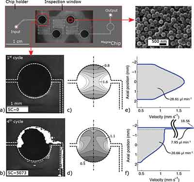
Microreactor Array Device
Researchers from University of Arizona used: 150mm 675um+/-25um.
150mm (6 Inch) Silicon Wafer Inventory
| Item | Dia | Type | Dopant | Orient. | Res (Ω-cm) | Thick (μm) | Polish | Grade | Description |
|---|---|---|---|---|---|---|---|---|---|
| 478 | 150mm | - | - | N/A | - | 650 | SSP | MECH | Low cost Si Wafer, great for spin coating. |
| 857 | 150mm | P | B | <100> | 0-10 | 620 | SSP | Test | Test Grade Silicon, great for studies. |
| 1025 | 150mm | N | - | <100> | 0-100 | 625 | SSP | Test | N-type Test Grade. |
| 2880 | 150mm | P | B | <100> | 0.006-0.012 | 525 | SSP | Test | With Oxide Back Seal. |
| 3071 | 150mm | P | B | <100> | 1-100 | 500 | SSP | Test | 2 SEMI-STD FLATS. |
| 1383 | 150mm | Undoped | - | <100> | >10,000 | 650 | SSP | Prime | Float Zone (FZ), High Resistivity. |
| 2476 | 150mm | N/P | - | <100> | 2k-10k | 675 | SSP | Prime | Float Zone (FZ). |
| 2312 | 150mm | P | B | <100> | 0.01-0.02 | 675 | P/E | EPI | With EPI layer. |
| UW1972 | 150mm | N | Phos | <100> | 2000-8000 | 320 | P/E | Prime | Float Zone (FZ), Thin. |
| E870 | 150mm | N | Phos | <111> | 0.001-0.014 | 605 | P/P | Prime | Double Side Polished (DSP), FZ. |
Available Dopants
- Boron Doped Silicon
- Antimony Doped Silicon
- Arsenic Doped Silicon
- Undoped Silicon
- Gallium Doped Silicon