Ultra-Thin Silicon for Increased Solar Efficiency
Thin silicon wafers used in solar panels have a few advantages over the standard 160 μm wafers.
- The thinner wafers allow more light to be absorbed, so less silicon is needed to make the same amount of electricity.
- The thinner wafers are easier to make, so they cost less and take less time to make.
- The thinner wafers are cheaper, so the electricity they make is cheaper.
50 μm wafers substrates could potentially reduce the cost of fabricating solar panels capex by 48%, module cost by 28%, and LCOE by 24%.
Get Your Quote FAST! Or, Buy Online and Start Researching Today!
New Process to Fabricate Ultra-Thin Silicon Wafers
UniversityWafer, Inc. and our partners have developed a new process for producing ultra-thin silicon wafers that can be processed with standard semiconductor equipment on flexible substrates. To provide a more flexible substrate for the production of ultra-thin semiconductors, we have started to produce thicker silicon rings to support ultrasonic wafers. We develop new processes for the production of thin-ring silicon with a thickness of less than 1 micrometer (micrometer) and a diameter of only 1 mm.
What Silicon Wafer Should I use to Fabricate MEMS For Drug Delivery
Scientists have used the following substrate spec to fabricate silicon-based MEMS vibrating mesh nebulizer for inhaled drugs.
100mm Undoped (100) 75um DSP
Scientists use the spec above to fabricate a silicon mesh for atomizing liquid.
Please contact us for pricing.
Physical Etch Masks for Plasma FIB
Researchers have used the following ultra-thin silicon wafers to fabricate their masks.
Researcher:
I’m looking to use these as physical etch masks for my plasma FIB. I’ve been told 100 um thickness works well, I’m curious to see if thinner gives similar results. As far as other specs, I just need material to get in between the Xe ions and my sample. I’ll take whatever you’ve got.
UniversityWafer, Inc. Quoted:
Prices would depend on the quantity and other specs. Single side polished is also available.
2" wafers 100 um thick,Both sides polished
2" wafers 75 um thick,Both sides polished
2" wafers 50 um thick,Both sides polished
3" wafers 100 um thick,Both sides polished
3" wafers 75 um thick,Both sides polished
3" wafers 50 um thick,Both sides polished
Ultra-Thin Silicon Wafers for Carbon Nanotubes
A professor requested a quote for the following research:
I have a PhD student who is trying to finish up and she needs to do a few trial runs of CVD growth of Carbon Nanotubes on a flex substrate and do some optical measurements after that. I am trying to get her a few pieces of flexible silicon to wrap up her thesis.
So, I technically don't even need a full wafer. Pieces would do. A broken wafer. Anything like that so that it is affordable to me.
Key Terms: Nanocellulose, carbon nanotubes, graphene, interaction, surface charge, conductivity, counterions
UniversityWafer, Inc. Quoted
Thin Si Item #3728
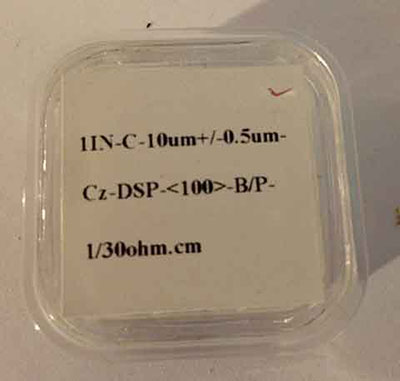
25mm P/B <100> 10um DSP Prime
Reference #267931 for pricing
We have a large Selection of Ultra-Thin Silicon Wafers
What are ultra-thin silicon wafers? Wafers with a thickness of 200 micron of thinner use the following for their thinning process mechanical grinding, stress reduction, polishing and etching. Presently and in the future ultra-thin silicon are important building blocks for the manufacture of semiconductor devices. Due to the special mechanical properties of ultra-thin wafer production, the handling of these wafers differs from the conventional one. Due to the rise of taiko wafers, special devices and carriers have the potential to eliminate ultra-thin wafer handling. Advances in ultra-thin wafer technology, manufacturing process, wafer transport and device applications are reviewed here.
Ultra-thin wafers have wide applications in semiconductor device manufacturing and will have long-term implications for the semiconductor industry.
Below are just some of the thickness wafers that we have in stock:
- 5 micron
- 10 micron
- 20-25 micron
- 50 micron
- 75 micron
- 100 micron
Other wafer thicknesses are available.

Thin Silicon Increases Solar Panel Efficiency
Climate change (formally referred to as global warming) is the greatest problem earth faces today. Scientists are urgently researching how to transition to a carbon-neutral energy system using the sun’s solar rays. Using current technologies, scientists have proven that the thinner the solar panel the greater the overall efficiency of production and solar capture. UniversityWafer, Inc. has assisted scientists in their quest for thin-silicon used to fabricate solar modules.
Thin Diamond Wire Sawed (DWS) Silicon Wafers
A research scientist requested the following quote:
I need thin Diamond Wire Sawed (DWS) silicon wafers of good quality (100) p-type and 4 inches in size. Please let me know how THINNEST you can provide, as I need the thickness of DWS wafers to be around 150um. Looking forward to hearing from you.
UniversityWafer, Inc. Quoted:
156mm x 156mm 150 ±10um N/Ph [100] ±3° Lapped 1-7 ohm-cm PSQ (Pseudo-Square), PV, Coin-roll packed in a group of 74 wafers (smaller Qty at higher price)
Researcher followed up:
Well, I think it will work. Actually we need wafers urgently but I need my professor's approval on this. Can you please send me the formal quotation?
However, I have a few doubt/queries as follow, please help me in this:-
1. what is PSQ (Pseudo-Square), PV, Coin-roll packed? - I don't understand this because I'm looking for diamond wire sawn (DWS) wafers (the wafers we get from the ingot before polishing etc)
2. Do you have p-type? - because I'm little more interested in single crystal p-type DWS silicon wafers (Though you can still send the quotation for n-type in case p-type is not available)
3. I need one box of silicon wafers i.e. 25 pieces in quantity.
4. Also, will it be possible for you to share me a picture of the wafer you mentioned above (if it's possible)
UniversityWafer, Inc. Responded:
Q1. what is PSQ (Pseudo-Square), PV, Coin-roll packed? - I don't understand this because I'm looking for diamond wire sawn (DWS) wafers (the wafers we get from the ingot before polishing etc)
A1. PSQ means "pseudo-square" and the acronym describes the wafer's shape, which is square with the corners cut-off (please see the picture). The wafers are DWS but also lapped after slicing to remove the damage layer occurred after the sawing.
Q2. Do you have p-type? - because I'm little more interested in single crystal p-type DWS silicon wafers (Though you can still send the quotation for n-type in case p-type is not available)
A2. No, we do not
Q3. I need one box of silicon wafers i.e. 25 pieces in quantity.
A3. These wafers are coin roll packed. We offer 25 pieces of item #7201 for $ /wafer.
Q4. Also, will it be possible for you to share me a picture of the wafer you mentioned above (if it's possible)?
A4. Here is a photo:

