What Is Gallium Nitride on Sapphire?
Gallium Nitride (GaN) on sapphire consists of a GaN epitaxial layer grown on a single-crystal
sapphire, or Al2O3, substrate. This material platform is widely used for LEDs,
laser diodes, ultraviolet detectors, RF devices, power electronics, and High-Electron-Mobility Transistors.
GaN is a
wide-bandgap semiconductor
with a direct bandgap of approximately 3.4 eV. Its high breakdown-field capability, fast electron transport,
and resistance to elevated operating temperatures make it attractive for high-frequency, high-power,
and optoelectronic device research.
Sapphire provides a durable and economical foundation for GaN
epitaxial growth.
It is especially common in blue, green, violet, and ultraviolet light-emitting devices.
Why Choose GaN on Sapphire Wafers?
Researchers select GaN-on-sapphire wafers for applications requiring:
- High-voltage device operation
- High-frequency switching
- Blue and ultraviolet light emission
- RF and microwave power amplification
- Resistance to elevated operating temperatures
- Custom doped and undoped GaN epitaxial layers
- Thin films for photonic and nanostructure fabrication
UniversityWafer can supply UID, silicon-doped, and magnesium-doped GaN structures with different wafer diameters,
layer thicknesses, substrate orientations, polishing options, and characterization data.
Get Your GaN on Sapphire Quote FAST! Or,
Buy GaN on Sapphire Wafers Online
and start researching today.
Available GaN Wafer and Template Options
UniversityWafer can help researchers source multiple gallium nitride material platforms, including:
- GaN on sapphire epitaxial wafers
- GaN/AlN on sapphire structures
- UID GaN templates
- Si-doped n-type GaN
- Mg-doped p-type GaN
- AlGaN/GaN HEMT structures
- GaN on silicon wafers
- GaN on silicon carbide
- Freestanding and bulk GaN substrates
- Nonpolar and semipolar GaN pieces
Researchers comparing substrate platforms may also review
silicon carbide wafers,
sapphire wafers,
and
AlGaN/GaN structures.
Research Example: Bulk and Freestanding GaN
A researcher requested information about a 2-inch bulk GaN wafer with an approximate thickness of 350 µm.
Their requested characterization included:
- Residual carrier concentration
- Dislocation density
- Surface polarity
- Macro-defect information
- Technical growth method
Related available material options included:
- 2-inch n-type bulk GaN wafer, approximately 350 µm thick
- 4-inch UID GaN template, approximately 4 µm GaN
- Nonpolar A-plane freestanding GaN pieces, approximately 350 µm thick
When requesting bulk or freestanding GaN, specify the required polarity, orientation, electrical type,
carrier concentration, thickness, size, defect limits, and quantity.
GaN Structures for HEMT Fabrication
GaN HEMT research typically requires a precisely defined epitaxial stack. Depending on the device design,
available structures may include:
- AlN on sapphire
- UID GaN on sapphire
- Si-doped GaN on sapphire
- Mg-doped GaN on sapphire
- AlGaN/GaN on sapphire
- AlGaN/GaN on silicon
- AlGaN/GaN on silicon carbide
For HEMT structures, provide the desired substrate, wafer size, buffer thickness, AlN nucleation layer,
AlGaN composition, barrier thickness, GaN thickness, doping, surface roughness, bow, warp, and quantity.
Example GaN-on-Silicon HEMT Request
A researcher requested the following epitaxial stack:
- UID GaN: 4–5 µm
- AlGaN transition layer
- AlN nucleation layer
- Silicon <111> substrate
- Low-roughness epitaxial surface
A related structure was available on 100 mm, 150 mm, and 200 mm silicon <111> wafers,
with an epitaxial surface roughness of approximately 0.5 nm or less.
GaN Wafers for Nanophotonics
Thin GaN layers on sapphire can be used for nanophotonics, photonic crystals, resonators,
waveguides, metasurfaces, and optical-device fabrication.
Example Nanophotonics Specification
- 100 mm diameter
- UID GaN on SSP sapphire
- GaN thickness: 100 nm or 150 nm
- Quantity: 15 wafers
Researchers working on thin-film optical structures should include target thickness tolerance,
orientation, roughness, usable surface area, wafer bow, and required optical characterization.
GaN for LEDs and Optical Devices
Because GaN is a direct-bandgap material, it is widely used in blue, violet, and ultraviolet
optoelectronic devices. Available structures may support research involving:
- Blue and green LEDs
- UV LEDs
- Violet laser diodes
- UV photodetectors
- Micro-LED displays
- Optical sensors
- Photonic integrated devices

GaN Measurement and Characterization Data
Measurement reports may be available for selected wafers for an additional charge.
Available characterization can include:
- Double-crystal X-ray diffraction rocking curves
- Room-temperature Raman spectra
- Photoluminescence mapping
- Atomic force microscopy at 5 × 5 µm or 20 × 20 µm scan areas
- Surface roughness data
- Hall-effect measurements
- Carrier concentration and mobility
- Bow, warp, and TTV measurements
Reference #115733 when asking about measurement services and pricing.
What Are Semi-Insulating GaN Applications?
Semi-insulating GaN is used when electrical isolation and low parasitic conduction are important.
It is commonly investigated for high-frequency and high-power device structures.
RF and Microwave Devices
- HEMTs: RF power amplifiers for radar, satellite communications, and wireless systems.
- MMICs: Monolithic Microwave Integrated Circuits for high-frequency electronics.
- Low-noise amplifiers: Signal amplification with reduced electrical interference.
High-Power Electronics
- Power amplifiers
- Switch-mode power supplies
- Power converters
- Automotive and electric-vehicle electronics
Optoelectronics and Photonics
- UV detectors
- Blue and UV LEDs
- Optical sensors
- High-speed photonic devices
GaN on Sapphire Wafers for RF, LED and Power Device Research
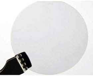 Gallium Nitride (GaN) on sapphire wafers combine a wide-bandgap GaN epitaxial layer with a durable and cost-effective
sapphire substrate.
This material platform is widely used to fabricate light-emitting diodes, laser diodes, ultraviolet photodetectors, RF components,
High-Electron-Mobility Transistors (HEMTs), and other high-frequency or high-power semiconductor devices.
Gallium Nitride (GaN) on sapphire wafers combine a wide-bandgap GaN epitaxial layer with a durable and cost-effective
sapphire substrate.
This material platform is widely used to fabricate light-emitting diodes, laser diodes, ultraviolet photodetectors, RF components,
High-Electron-Mobility Transistors (HEMTs), and other high-frequency or high-power semiconductor devices.
UniversityWafer supplies GaN-on-sapphire epitaxial wafers with multiple wafer diameters, GaN layer thicknesses,
doping options, crystal orientations, and polishing configurations. Available structures may include unintentionally doped GaN,
silicon-doped n-type GaN, magnesium-doped p-type GaN, AlN nucleation layers, and custom
epitaxial layer stacks.
Send us your required diameter, layer structure, doping, GaN thickness, sapphire thickness, orientation, polish, quantity,
and characterization requirements. We can help identify an available wafer or provide a custom quotation.
Why Use Gallium Nitride on Sapphire?
GaN is a direct-bandgap III–V semiconductor with a bandgap of approximately 3.4 eV. As a
wide-bandgap semiconductor,
GaN supports high electric fields, elevated operating temperatures, and high-frequency device operation.
Sapphire provides an established foundation for GaN epitaxy, particularly for optoelectronic and RF research.
Researchers select GaN on sapphire for applications such as:
- Blue, green, violet, and ultraviolet LEDs
- Laser diodes and optical emitters
- UV photodetectors and optical sensors
- RF and microwave power amplifiers
- GaN HEMTs and transistor development
- 5G and millimeter-wave device research
- High-temperature electronic devices
- Nanophotonics and integrated photonics
- Radiation-tolerant semiconductor research

Available GaN Epitaxial Platforms
The substrate and buffer structure should be selected according to the intended device, thermal requirements, wafer diameter,
and fabrication process. Commonly requested configurations include:
-
GaN on Sapphire: GaN epitaxial layers grown on c-plane Al2O3 for LEDs,
photodetectors, optical devices, RF research, and general GaN device fabrication.
-
GaN/AlN on Sapphire: An AlN nucleation or buffer layer between the GaN film and sapphire substrate
to support epitaxial growth and device-layer engineering.
-
GaN on Silicon Carbide: GaN deposited on
SiC substrates
for applications requiring improved heat dissipation and high RF power density.
-
GaN on Silicon: GaN epitaxial structures on
silicon wafers
for larger-diameter processing, device prototyping, and semiconductor fabrication research.
-
AlGaN/GaN Structures:
AlGaN/GaN epitaxial wafers
for HEMTs, RF devices, sensors, and high-power transistor development.
GaN on Sapphire Wafer Specifications
The table below presents examples of previously available GaN-on-sapphire wafer configurations.
Inventory may change, and additional diameters, doping levels, film thicknesses, and layer stacks may be available upon request.
| Item |
Diameter |
Type/Doping |
Orientation |
GaN Thickness |
Sapphire Thickness |
Sapphire Plane |
Polish |
Additional Specifications |
| 2859 |
100 mm |
N-type / Si-doped |
<0001> |
5.0 µm |
650 µm |
C-plane |
DSP |
Contact us to confirm current availability. |
| 2521 |
50.8 mm |
N-type / Si-doped |
<0001> |
5.0 µm |
430 µm |
C-plane |
DSP |
Suitable for research and device fabrication. |
| 2857 |
50.8 mm |
P-type / Mg-doped |
<0001> |
4–5 µm |
430 µm |
C-plane |
DSP |
Usable surface area >90%; TTV ≤10 µm; bow ≤10 µm; warp ≤10 µm. |
| 2856 |
50.8 mm |
P-type / Mg-doped |
<0001> |
4–5 µm |
430 µm |
C-plane |
SSP |
Contact us for characterization data and quantity options. |
Abbreviations: UID means unintentionally doped, DSP means double-side polished,
SSP means single-side polished, and TTV means total thickness variation.
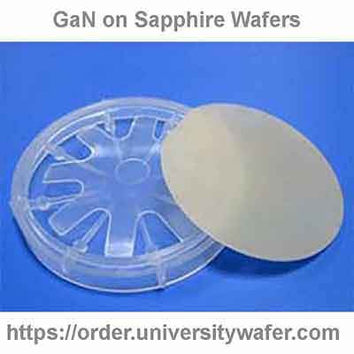
The image above shows a 50.8 mm GaN-on-sapphire wafer supplied in a single-wafer carrier.
Ask about SSP or DSP surfaces, wafer carriers, measurement reports, strained heteroepitaxial growth,
and epitaxial overgrowth options.
Choosing GaN Doping and Layer Thickness
The correct doping and GaN thickness depend on the intended device structure.
UniversityWafer can help researchers compare the following options:
-
UID GaN: Commonly requested for buffer layers, optical studies, photodetectors,
transistor development, and research requiring low intentional doping.
-
Si-doped GaN: Used when an n-type conductive GaN layer is required.
-
Mg-doped GaN: Used to produce p-type GaN for LEDs, junction devices, and related optoelectronic structures.
-
Thin GaN films: Nanometer-scale GaN layers may be requested for nanophotonics,
metasurfaces, optical resonators, and thin-film device research.
-
Thicker GaN layers: Micron-scale films are commonly selected for device fabrication,
electrical characterization, etching, and epitaxial process development.
GaN on Sapphire for HEMT Research
High-Electron-Mobility Transistors use a heterostructure that creates a high-mobility electron channel near the interface
between semiconductor layers. Researchers developing a
GaN transistor
or HEMT may request an AlGaN/GaN stack, an AlN nucleation layer, a UID GaN buffer, and specific cap or barrier layers.
Example HEMT-related platforms include:
- AlGaN/GaN on sapphire
- AlGaN/GaN on silicon carbide
- AlGaN/GaN on silicon <111>
- UID GaN with AlGaN transition layers
- GaN layers with AlN nucleation or buffer layers
- Custom epitaxial structures for RF and power transistors
When requesting a HEMT structure, include the desired substrate, wafer diameter, GaN buffer thickness,
AlGaN composition and thickness, AlN thickness, doping, cap layer, surface roughness, bow, warp, and quantity.
GaN Wafers for RF and Microwave Devices
GaN is frequently investigated for RF power devices because its material properties support high electric fields,
high-frequency switching, and high power density. Potential device applications include:
- RF power amplifiers
- Microwave and millimeter-wave circuits
- Radar and communication systems
- RF front-end modules
- Schottky barrier diodes
- 5G and wireless communication devices
For RF applications requiring improved thermal performance, researchers may compare GaN on sapphire with
silicon carbide wafers.
For larger-diameter process development, GaN-on-silicon structures may also be considered.
Research Example: GaN for an RF Schottky Barrier Diode
A researcher requested a GaN substrate for an RF Schottky Barrier Diode (SBD) application.
One proposed configuration was:
- 100 mm GaN-on-silicon wafer
- Quantity: 10 wafers
- Application: GaN RF Schottky Barrier Diode fabrication
Contact UniversityWafer and reference #262996 when requesting related specifications or updated pricing.
GaN on Sapphire for LEDs and Photonics
 GaN-on-sapphire is an established material platform for visible and ultraviolet optoelectronics.
Its direct bandgap makes it suitable for light emission, while alloying GaN with indium or aluminum
allows researchers to engineer optical and electronic properties for different wavelength ranges.
GaN-on-sapphire is an established material platform for visible and ultraviolet optoelectronics.
Its direct bandgap makes it suitable for light emission, while alloying GaN with indium or aluminum
allows researchers to engineer optical and electronic properties for different wavelength ranges.
GaN photonic and optoelectronic applications include:
- Blue and green LEDs
- Violet and ultraviolet laser diodes
- UV photodetectors
- Optical sensors
- Micro-LED and display research
- Nanophotonic resonators
- Integrated photonic devices
- Optical and electrical characterization studies
Research Example: Thin GaN for Nanophotonics
Researchers developing GaN nanophotonic structures requested thin GaN layers on sapphire with thicknesses of
approximately 100 nm and 150 nm. A related configuration included:
- 100 mm diameter wafer
- Unintentionally doped GaN
- SSP sapphire substrate
- GaN thickness: 100 nm or 150 nm
- Quantity: 15 pieces
Custom thin-film GaN wafers may be suitable for nanophotonics, optical metasurfaces,
waveguides, photonic crystals, resonators, and etching studies.
GaN Material Characterization
Characterization data may be available for selected GaN-on-sapphire wafers.
When requesting a quote, ask whether reports are available for:
- X-ray diffraction (XRD)
- Rocking-curve full width at half maximum (FWHM)
- Atomic force microscopy (AFM)
- Surface roughness
- Photoluminescence (PL)
- Raman spectroscopy
- Hall-effect measurements
- Carrier concentration and mobility
- Resistivity or sheet resistance
- Bow, warp, and total thickness variation
- Usable surface area and defect information
Example Mg-Doped GaN Data
Previously supplied Mg-doped GaN-on-sapphire material included the following representative values:
- FWHM of the symmetric (002) rocking curve: approximately 250 arcsec
- FWHM of the (102) rocking curve: approximately 300 arcsec
- Mg concentration: greater than 6 × 1016 cm−3
- Resistivity: approximately 10 Ω·cm
Related configurations included:
- 2-inch UID GaN/Al2O3, 4–5 µm GaN, (0001), SSP
- 2-inch Mg-doped GaN/Al2O3, 4–5 µm GaN, (0001), SSP
Reference #257591 when requesting related specifications and pricing.
GaN on Sapphire Compared with Silicon
GaN and silicon serve different device requirements. Conventional
silicon
remains widely used because of its mature fabrication infrastructure, broad diameter availability, and cost-effective processing.
GaN is often selected when a device requires higher electric-field capability, higher-frequency operation,
or direct-bandgap optoelectronic performance.
| Selection Factor |
GaN |
Silicon |
| Bandgap |
Wide, approximately 3.4 eV |
Approximately 1.12 eV |
| Bandgap type |
Direct |
Indirect |
| Common strengths |
RF, power, LEDs, lasers and UV devices |
Integrated circuits, MEMS, sensors and established processing |
| Wafer availability |
Typically smaller and more specialized |
Broad selection of diameters and specifications |
| Fabrication ecosystem |
Specialized compound-semiconductor processing |
Highly mature and widely available |
The best substrate depends on device voltage, frequency, thermal design, optical wavelength, fabrication compatibility,
wafer diameter, budget, and required production volume.
How Is GaN Grown on Sapphire?
GaN layers are commonly deposited using
Metal-Organic Chemical Vapor Deposition (MOCVD)
or related vapor-phase epitaxy processes. Because GaN and sapphire have different lattice and thermal properties,
a nucleation or buffer layer—often AlN or low-temperature GaN—may be introduced before the primary GaN layer is grown.
A typical simplified GaN-on-sapphire structure may include:
- C-plane sapphire substrate
- AlN or GaN nucleation layer
- GaN buffer layer
- UID, Si-doped, or Mg-doped GaN device layer
- Optional AlGaN, InGaN, cap, quantum-well, or contact layers
Exact layer structures vary considerably between LED, HEMT, photodetector,
laser, sensor, and power-device applications.
Is GaN on Sapphire Resistant to Mineral Oil?
A researcher asked whether a GaN material sheet could be exposed to mineral oil.
GaN is generally chemically stable against nonpolar mineral oil under ordinary room-temperature conditions.
The more significant concern is surface contamination rather than immediate chemical attack.
Oil residue can interfere with later photolithography, thin-film deposition, wire bonding, electrical contacts,
or surface characterization. Researchers should establish a substrate-compatible cleaning process before exposure
and confirm that the cleaner will not damage existing metals, polymers, photoresists, coatings, or device layers.
Reference #434762 when requesting related specifications or pricing.
Request a GaN on Sapphire Wafer Quote
To receive an accurate quotation, provide as much of the following information as possible:
- Wafer diameter and quantity
- Sapphire orientation and thickness
- GaN thickness
- UID, Si-doped, or Mg-doped GaN
- Target carrier concentration or resistivity
- SSP or DSP surface finish
- Required AlN, AlGaN, InGaN, or buffer layers
- Surface roughness requirements
- Bow, warp, and TTV limits
- Required XRD, AFM, PL, Raman, or Hall data
- Device application or fabrication process
Related Wafers for GaN Device Development
Researchers evaluating GaN on sapphire may also need the following materials:
-
Sapphire Wafers
— bare Al2O3 substrates for epitaxy, optical devices, and thin-film deposition.
-
AlGaN/GaN Wafers
— heterostructures for HEMTs, RF electronics, and sensor research.
-
Silicon Carbide Wafers
— high-thermal-performance substrates for RF and power-device development.
-
Silicon Wafers
— substrates for GaN-on-Si growth, process development, controls, and semiconductor fabrication.
-
Gallium Arsenide Wafers
— compound-semiconductor substrates for RF, photonic, and optoelectronic research.
-
Thermal Oxide Wafers
— SiO2-coated silicon substrates for insulation, controls, and fabrication experiments.
