Sapphire Wafer Applications

university wafer substrates

Sapphire Wafers Transparent to Infrared Light

An opto-electronic engineer requested a quote for the following.

We need 200mm 1.0 mm thick Sapphire. We only need two wafers to test. One needs to be double side polished (optical grade) The other needs to be unpolished with a frosty appearance. We want the material to be transparent to infrared light down to the wavelength of 5 microns.

Reference #209328 for specs and pricing.

Why Use Sapphire Substrates?

Sapphire substrates are notable for their well-defined optical constants, which refer to its refractive index and extinction (absorption) coefficient. These parameters determine how light interacts with the sapphire material, including how much light is absorbed, reflected, or refracted.

Sapphire Al2O3 Refractive Index

Sapphire substrates have excellent transparency in a wide wavelength range from UV to IR. They have a high refractive index (about 1.77 in the visible light range) which makes them beneficial in a variety of applications where light manipulation is needed. They are also incredibly durable and resistant to physical damage and chemical corrosion.

Applications that utilize these unique optical properties range from LED production, to optical components in various electronics, to the production of components for high-powered lasers.

Please note that these optical constants can be influenced by the quality and treatment of the sapphire substrate, including factors such as the purity of the sapphire, the crystallographic orientation, and any post-growth treatments that the sapphire undergoes.

What is the Easiest Sapphire Plane to Cleave?

How we help Scientists:

A researchers asked for a quote on 4" and 6" Sapphire substrates (BUY ONLINE):

I will be used to pattern photoresists. As a result, substrates will be exposed to high temperatures (up to 200oC) as well as highly alkaline solutions (pH>12). They will also need to withstand multiple reworks (re: strip photoresists and re-use of substrate many times).

Answer:

Plane (C)= C-plane sapphire is the softest for cleave

Reference #199562 for specs and pricing.

Researchers rejoice! We have a large inventory of sapphire substrates in stock. Below is just a few of what's available. Some sapphire applications include:

Get Your Quote FAST! Or, Buy Sapphire online and start researching today!


Sapphire Wafer Packaging

Please see below for how very secure our sapphire wafer packaging is. 2 spring (claw) on (Spring 2# ) and below (Spring 1#)the wafer to hold the wafer no shifting in the box. 

wafer packaging for sapphire substrates

Typical Single Wafer Carrier

Sapphire Semiconductor Substrates are available in all Orientations

Orientations include

Sapphire substrates are available in various shapes (circular, rectangle, or square), from a few mm up to 200mm in size, and finishes according to customer specification. Primary flats(as per industry standards) are provided on circular substrates for orientation purposes; secondary flats are available on request. Substrate thickness' range from 0.013" (0.25mm) to 0.025" (0.675mm), depending on your particular application requirements.

Sapphire Substrate Price

Sapphire semiconductor substrates are manufactured at Sapphire Products from high quality optical grade Czochralski sapphire. UniversityWafer's integrated facilities allow regulation of the production of substrates from crystal growth to fabrication, and to accommodate special requests on very short notice.

We have sapphire wafers in stock!

sapphire wafer inventory

The sapphire wafers have a high purity >99.996%. See below for impurity analysis for Al2O3 sapphire windows.

sapphire wafer purity

Sapphire Wafers for Cryogenic Design

Researcher:

As we are working on cryogenic design. Could you please provide thermal behavior and data file for the sapphire substrate so that we can simulate and use in the fabrication.

UniversityWafer, Inc. Replied:

Pls see below for all the property of the sapphire wafer

" Dielectric properties and optical properties :
Sr. No. Property Value
1 Material 99.996% pure Al2O3 (Alumina)
2 Material class according to DIN EN 60672 C795
3 Density 3.73 g/cc
4 Coefficient of thermal expansion
100° – 200° C 6.0 – 8.0 * 10 -6 /K
100° – 300° C 6.0 – 8.0 * 10 -6 /K
100° – 600° C 6.7 – 8.7 * 10 -6 /K
100° – 800° C 7.0 – 9.0 * 10 -6 /K
5 Dielectric constant (10 MHz to 1 GHz) 8.3 – 11.3
6 Dielectric loss factor (10 MHz to 1 GHz) ≤ 5 * 10 -3
7 Breakdown field ≥ 15 kV/mm
8 E-Modulus ≥ 300 GPa
9 Thermal conductivity at 20° C ≥ 22 W/m K
10 Volume resistivity at

20° C ≥1013 Ω-cm
200° C ≥1011 Ω-cm
400° C ≥109 Ω-cm
600° C ≥107 Ω-cm
11 Water absorption ≤ 0.1%

12 Light transmission characteristics: T>/=80% (0.3~5μm)

What is Sapphire Thermal Conductivity?

Sapphire has a thermal conductivity of approximately 46-50 watts per meter-kelvin (W/m·K) at room temperature. This thermal conductivity value indicates that sapphire is a relatively efficient conductor of heat.

Sapphire optics can withstand elevated temperatures while efficiently transferring heat away from sensitive components. Its ability to conduct heat effectively helps dissipate heat generated thus preventing overheating and maintaining their performance and reliability makes sapphire an excellent choice for high-power electronic devices and semiconductor components.

Overall, sapphire's thermal conductivity is an advantageous property for applications where efficient heat transfer and management are necessary.

What is the refractive index of sapphire?

Refractive index: no =1.768 ne =1.760

How Do You Cut a Sapphire Window?

Sapphire is an incredibly hard crystal. It has excellent chemical and thermal resistance. It is also scratch resistant. The crystalline structure makes it easier to cut than other crystals, and the random orientation of a sapphire window allows you to achieve any desired pattern. These windows are also much thinner than other types of windows, and can operate at temperatures up to 20300C. But, how do you cut a sapphire window in a symmetrical way?

Sapphire is a birefringent, flat, transparent material. To cut it properly, it should be cut along a zero-degree plane, such as the C-Cut. You can also cut it at a random angle to get the best colour and brilliance. The sapphire's transmittance is also improved, so cutting it at a random angle isn't advised. Its ability to resist UV radiation is another benefit.

Unlike diamonds, sapphires are extremely resistant to UV light. Even in sunlight, sapphire will not darken. This means that they can be used in a wide variety of applications. In addition to its durability, sapphire windows can also be thin. In order to create a symmetrical cut, you must make sure that the sapphire isn't distorted or broken.

Sapphire is an optical window - a transparent window made of a hard mineral called sapphire. Because of its transparency, it is highly resistant to shock and is birefringent. In addition to use in high-tech applications, it is a popular choice for optical windows in harsh environments. Additionally, it is widely used for femtosecond lasers in broadband continuum generation.

Sapphire windows are hard and durable, and can withstand high-energy lasers. Because of its optical properties, sapphire windows are thinner than other windows. They can also be cut into random shapes. The shape of a sapphire window will depend on the orientation of the crystal. Regardless of how they are cut, they can be asymmetrical and will help improve the appearance of a room.

The sapphire window is different from any other window. It is not available in a standard cut, and sapphire windows are made using a custom method. They are asymmetrical, meaning that they are flat and parallel to each other. This makes them more expensive, but this makes them stronger and more durable. They will not darken if they are exposed to UV light, and are also much thinner than other types of windows.

Optical Grade. Sapphire is the most expensive type of window. This type of sapphire will not darken due to UV radiation, but will still reflect light and be opaque to light. Because it is transparent, the sapphire window will be able to pass the most amount of light, so it will be the perfect choice for any room. They will also make any room look more beautiful.

Optical Grade: The cut of a sapphire window is crucial. The grade should be optical, but it is important to make sure the glass is cut at the correct orientation. It will not be distorted if you have a perfect angle. If you want a more symmetrical window, you need to use the proper angles. If you are aiming for a symmetrical sapphire window, you need to follow the symmetry of the cut.

Sapphire is a beautiful material that has a unique set of properties. It is one of the most durable crystals. It is also one of the hardest stones in the world. As a result, a sapphire window can be made of different types of materials, and is therefore more expensive. The most common type of sapphire windows are optically-graded. The optical grade is the best choice for any sapphire.

When it comes to sapphire, you should know that it is possible to find a sapphire with a window. A small sapphire with a small window will be more difficult to cut, but it will make the stone look much larger than a sapphire with a larger-quality window. It is important to note that a window is not the same as a sapphire with a large-scaled face.

What is Microroughness of Sapphire Wafer Surface?

The surface roughness of sapphire is a critical factor to the performance of light-emitting devices. This is due to the fact that sapphire is very susceptible to various types of ionizing radiation and charged particles. To further improve the performance of light-emitting devices, it is imperative to optimize the surface preparation of the substrate. Furthermore, the microroughness of sapphire is affected by external action, including the etching process.

sapphire wafer surface microroughness

To better understand sapphire microroughness, we first looked at the CL spectra of original and heat-treated sapphire samples. This method revealed that the A-plane sapphire had the highest surface roughness after chemical-mechanical polishing, while the C-plane sample had the lowest. The low F+-band intensity was associated with high surface roughness, and this correlated with the generation of oxygen vacancies.

Moreover, the surface microroughness of sapphire was studied through a chemical etching process. In this process, aluminum atoms were reduced to form nanocrystals and then diffused to the negatively charged gold islands. Hence, the negative charge derived from the sapphire surface was minimized, and this contributed to the continuity of the etching process. Moreover, the flow of aluminum atoms to the gold nanocrystal increased its size and rounded shape at the base region. The presence of aluminum atoms on the surface of the sapphire microroughness could also cause the accumulation of compounds of the Al-Au system.

The degree of sapphire microroughness is largely dependent on the type of machining technique used. Machined sapphire has excellent mechanical, optical, and thermal properties, and it is the material of choice for high-performance systems. However, sapphire is a difficult material to machine. Typically, the most common methods of cutting sapphire are grinding and laser machining. Understanding how sapphire breaks down is essential to optimizing processing parameters.

Growing ZnO Film on Sapphire Substrates

A postdoc requtesed a quote on the following:

Hi, Would you be able to send me a quote for the following ZnO Epi Film on Sapphire wafers. 1) ZnO Film (0.5 um) on Sapphire(0001), 10x10x0.5mm,SSP , undoped, Qty: 01 2) ZnO Film (0.5 um) on Sapphire(0001), 5x5x0.5mm ,SSP, undoped, Qty: 01 3) ZnO Film on Sapphire(0001), 2"x0.5mm, undoped , ZnO: 0.5 um, Qty: 01.

UniversityWafer, Inc. Quoted

ZnO Epi Film on Sapphire wafers.

  1. ZnO Film (0.5 um) on Sapphire(0001), 10x10x0.5mm,SSP , undoped
  2. ZnO Film (0.5 um) on Sapphire(0001), 5x5x0.5mm ,SSP, undoped
  3. ZnO Film on Sapphire(0001), 2"x0.5mm, undoped , ZnO: 0.5 um

Reference # 252990 for pricing.

What Sapphire Substrate Diameters are Available?

We have a large selection of stadard diameters and custom dimension availble. Please send us your specs or click below:

What is Sapphire Substrate?

Sapphire substrates is extremely hard and durable. Applications include semiconductors, solar cells,sapphire wafer appearance and blue LEDs. Sapphire's s distinct properties that make it an excellent choice for many types of applications.


Sapphire is a common material used to make crystals. It is used in electronics, including in the production of lasers and in IR detectors. The substance is also widely used in electronic devices, including refrigerators and washing machines. Integrated circuits are a major component of most electronic devices today. As these technologies continue to grow and become more complex, the need for high-quality sapphire substrates will only increase.

The use of sapphire substrates in electronics is almost endless. Its thermal and electrical shock resistance makes it an excellent window material. The material is also resistant to sand erosion. Its excellent optical insulation makes it an excellent choice for many applications. Because of its high-temperature resistance and high scratch resistance, sapphire is also used to grow heteroepitaxial silicon in microelectronic ICs. Its properties and applications are endless and will only increase in the future.

Sapphire substrates are available at a wide variety of prices. It has a high thermal conductivity, is resistant to water and sand erosion, and has many other properties that make it a superior window material. These qualities make sapphire a preferred material for semiconductor chips.

Despite the high cost of sapphire substrates, this material is a valuable commodity. It is used for a variety of applications. For example, it is used for IR detectors, and it has been used in blue LEDs. Moreover, it is resistant to heat and sand erosion. Its high thermal conductivity makes sapphire substrates an excellent choice for use in many electronic devices.It is a material that is made of sapphire and has a combination of properties. It is resistant to high temperatures, sand erosion, and chemical reactions. It also has a high thermal conductivity and resists scratching. The advantages of using sapphire for electronic devices are many. It is also a great choice for the manufacturing of solar panels, LEDs, and other electronics.sapphire wafers

The sapphire substrate is a unique material that has a unique combination of properties. Its high thermal resistance to water and sand make it a desirable material for the construction of electronic devices. Its low thermal conductivity makes it a desirable material for solar and other solar panels. In addition, the sapphire substrate is a valuable resource for many industries.

There are a variety of sapphire substrates on the market. It is an ideal material for semiconductor applications. It is resistant to water, heat, and sand erosion, and it is a great material for IR applications. It is also a good thermal conductor, so it can be used in a wide range of devices. It is also a valuable material for electronics, and NASA uses it in many areas.

In addition to semiconductors, sapphire substrates are used in other applications. For instance, the semiconductors used in computers are often found in televisions, refrigerators, washing machines, and LED bulbs. There is also a significant market for these materials in the semiconductor industry. Regardless of its popularity, the sapphire substrates will continue to grow and be used in an ever-increasing variety of applications.

A sapphire substrate can be a good option for semiconductors. A sapphire substrate can be used to form GaN or other thin films. It can be made from raw materials or from sapphire. Typically, the sapphire substrate is made of pure sapphire. The material is very hard and can be broken into smaller pieces, which is very useful in making electronics. Once the process has begun, the semiconductor will be installed, and the finished product will look like a crystal.

What is Sapphire Thermal Conductivity

The properties of sapphire vary depending on its orientation. Its linear thermal expansion coefficient is large at room temperature, but it is poor in terms of its resistance to thermal shock. A sample of ph50x3t (mm) on the c-plane was subjected to a test in which it was immersed in 10degC water. The result: No cracks were detected until a temperature of 200degC, and cracks were detected at 250degC.
Thermal conductivity measurements are performed by using multiple-detector IR cameras. IR measurements are similar to observations at the visible spectrum. In this study, an IR camera with a 256x256 Indium-Antimonide detector array was used to measure the radiation intensity at the rake face. The IR images were recorded at different depths on the chip-tool interface.
IR cameras can image the entire interface between a chiptool and a wafer. Infrared measurements are similar to those made at visible wavelengths, but the process requires more precision. Using the IR camera with a multiple-detector spectrometer, the researchers were able to measure the intensity of radiation from the rake face of a sapphire wafer.
The resulting temperature contour plots are highly accurate, and they are based on current knowledge. However, there is no guarantee that the products described in these data sheets will not cause harm. As with any material, you should consult the manufacturer's safety data sheet for more information. This document provides general guidelines for handling the materials. If you are unsure of their safety, do not hesitate to contact the company.

Sapphire Wafer Optical Properties

Sapphire is a naturally occurring substance with exceptional optical properties. Because of its high crystalline structure, it is used in many semiconductor and other industrial applications. The main advantages of sapphire include its low transmitted wavefront distortion, chemical resistance, and surface hardness, second only to diamond. Because of these benefits, sapphire is widely used in semiconductor and other high-precision optical applications. Here are some of the most notable optical properties of sapphire.
Sapphire is a single-crystal aluminum oxide. It transmits wavelengths from 150 to 6000 nm, making it useful for many applications. Because of its strong and uniform optical properties, sapphire is often used in photovoltaic panels and other optical devices. The material is also highly durable and is often less expensive than asymmetrical sapphire. However, because of its unique physical properties, it should only be used for asymmetrical lenses.
The best sapphire wafers are made of a single crystal and are highly transparent. This material can be used for a variety of applications, from displays to lasers. The material's high crystalline structure makes it ideal for applications that require a narrow bandgap. This means sapphire will not be distorted when used in a spectrometer. It will remain perfectly clear even if exposed to intense ultraviolet light.

Sapphire Wafer Laser Diodes

The performance of Sapphire Wafer Laser Diodes is determined by their spectral properties and reliability. It is not uncommon to observe good reliability of these lasers at very high powers. However, reliability has been a limiting factor. The following section describes the key features of these diodes. The main advantages of these devices are detailed below: They are small, reliable and inexpensive. They also feature high power and high repetition rate.
The first major advantage of this laser type is its high average power and high efficiency. The Yb-doped Tourmaline Yb-SS diode has an average power of more than a Watt. This enables it to operate at over-micron wavelengths with a very high degree of accuracy. Yb-SS features a solid bulk body and an integrated pump diode module. The new laser is designed for UV, VIS, and NIR spectral regions.
Another major benefit of Sapphire Wafer Laser Diodes is their stability and flexibility. These lasers are made in different orientations. They can be either single- or dual-wavelength and double-pulsed. They are generally used in the manufacture of semiconductor devices. These lasers are highly stable. The crystalline structure of these diodes is quite high, and they can withstand temperatures of up to 1100 °C.

What is Sapphire Refractive Index

In order to determine the sapphire's refractive index, scientists measure the wavelength and temperature at which the material is transparent. These measurements are important in the velocity correction of laser interferometer experiments and for analyzing sapphire's high-pressure properties. They also show a possible approach to study shock transitions in transparent materials. This article discusses how the measurements are made and how to interpret the results. This article explains how to use the measurements for this purpose.
The sapphire's refractive index can be measured using an aplanatic point technique. This technique involves placing the sample on the aplanatic point of the spherical surface of the aNAIL, which produces an aberration-free focal spot. The aplanatic point technique is another method for calculating the aPlanatic angle of the spherical surface of an aNAI.
This method uses an immersion liquid to fill a gap between the immersion objective lens and the facing surface of the sample. The sample of interest is then suspended in the liquid. The present invention provides a new method for making sapphire immersion liquids and sapphire immersion objectives. This allows for the measurement of a sapphire's refractive index. The invention also enables a more accurate determination of the refraction index of an object.
The refractive index of a sapphire is dependent on the amount of iron present in the sapphire. A natural sapphire with a high level of iron may have a typical 450 complex that shows two clear lines at 450 and 460 nm and a third line at 470 nm. The 450 nm line will be more noticeable on a natural sapphire with a lower content of iron. This phenomenon is also observed in synthetic sapphires.

What is Sapphire Wafer Dielectric Constant

The single-crystal sapphire is an excellent insulator, microwave window, and semiconductor substrate. Its hexagonal crystal structure makes it an excellent choice for a variety of applications. The high-temperature properties of sapphire make it an ideal choice for a variety of industries, including the Electronics Industry. Furthermore, it offers a wide range of optical and thermal properties, and is one of the most resistant oxide crystals.
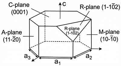
The C plane is 0.001 degree off the M plane, while the R-plane is 0.02-degree-off. The A-plane is 11-20 degrees, and the M-plane is 0.2-0.1 degrees off. A-plane sapphires have a dielectric constant of approximately 0.1-cm. However, sapphires have extremely high resistivity to thermal shock, which is why they're used in sensitive electronic components.
The dielectric constant of sapphire is very high, and it has a very low thermal conductivity. Its crystalline structure also means that it resists chemical reactions, makes it scratch-resistant, and is resistant to extreme temperatures. It also has a high thermal conductivity, making it a perfect window material for many IR applications. Because of its low thermal conductivity, sapphire wafers are often used for epitaxial silicon deposition and for HB-LED production.
One type of sapphire wafer is single-crystal. Its size ranges from one to six inches. Its unique properties make it a popular choice for electronic components. Its high anti-abrasion and corrosion resistance, low dielectric loss, and excellent insulating properties make it a popular choice for vacuum equipment. For vacuum-compressors, it is also used for vacuum systems.

What is Sapphire Wafers Surface Roughness

Chemical mechanical polishing (CMP) of sapphire wafers typically involves the use of toxic solutions, which are harmful to the environment. This makes developing a green CMP technique important. To combat environmental concerns, a new green CMP slurry was developed. The slurry included deionized water and dried by compressed air. The resulting sapphire wafers were inspected and tested for surface roughness.
The surface roughness of a sapphire wafer is an important factor when light emitting devices are being developed. High-quality sapphire substrates will help to minimize the loss of light during the light emission process. However, it is also essential to check the quality of the substrate and determine its smoothness to ensure that it will not cause any optical problems. The process of CMP is designed to determine how smooth or rough the sapphire wafer surface is and confirm whether it is low in haze or not.
A low-haze surface finish is critical for LED and laser components. This means that the surface roughness should be uniform, with minimal haze. In addition, the NCD substrate should have a rough surface and be flat. While it is difficult to predict the exact shape of the substrate, CMP will help determine its roughness and ensure that it is as smooth as possible. The roughness level of a sapphire wafer should be as low as possible.

What is Sapphire Wafer Crystal Structure

The sapphire wafer crystal structure is one of the most interesting in optical materials. The mineral is named corundum. Impurities such as iron and titanium give it its beautiful blue color. The best manufacturers of sapphire substrates include Cryscore. Here is a closer look at the sapphire wafer crystal structure. This material is extremely durable. Besides, it is a highly crystalline substance.
A sapphire wafer is a single crystal made of alumina. Its crystal structure is hexagonal. It can be used in the fabrication of photovoltaics, solar cells, and LEDs. In addition to this, sapphire is widely used for HB-LED production. It is also a low-power semiconductor and is resistant to thermal shock. However, sapphire wafers are not always perfect, and sometimes defects appear.
This crystal has excellent physical, chemical, and optical properties. Its single-crystal structure is the most stable of all the oxide crystals, and it retains its high strength and chemical resistance even at high temperatures. It is used in mobile devices and in many other electronic applications. The material's low thermal conductivity makes it ideal for electronics. So, if you're looking for sapphire wafers, contact us today. There are a number of companies offering these services and more.
The sapphire wafer crystal structure is an important research topic in epitaxy. This material is used to make micron-patterned LEDs. The luminous power of PSS-LEDs has increased by 30%. Moreover, it is a new substrate for solar cells. Ultimately, the sapphire wafer is a versatile substrate for LED production. You can use it as a carrier, bonding substrate, and window.

Is Sapphire a Semiconductor?

Are you wondering - Is Sapphire a semiconductor? The answer to this question is not so simple, and al203 semiconductorsthe answers will vary depending on what applications you're considering. In the case of RF, for example, Sapphire excels due to its high linearity, making it a good candidate for high-end RF switches. But in the broader market, the answer is yes. Listed below are the top five uses of this semiconductor.

High-purity sapphire crystals are used for Silicon-on-Sapphire SoS, which involves a deposition of silicon onto a heated sapphire substrate. The process is complicated and has the potential to cause uneven lattices in the crystal. In addition, p-type dopants such as aluminum are not well-suited for SoS, and result in disparities in crystal lattice. Hence, the question, "Is Sapphire a semiconductor?" is more aptly answered with a yes.

The sapphire technology market is fragmented, with well-diversified global vendors. The growth of global players is encouraging, but regional vendors are finding it difficult to compete with them. The report focuses on five key segments in the sapphire industry: RF, IC, and MMIC, as well as the ICT and consumer electronics segment. Further, the report provides analysis of all these segments, including revenue forecasts and trends.

How Are Sapphire Wafers Made?

Sapphire wafers are made by cleaving and grinding a crystal bar. During the cutting process, there how to fabricate sapphire wafersis a large amount of thermal and mechanical stress, which can cause a deep damage layer. After the cutting, the material undergoes a polishing step to increase its flatness and curvature. This step is done to eliminate the damage layer, which can cause cracks.

The final step in the process is to remove the excess material by using a scribe. To do this, a FlipScribe is used. The pliers are designed to make a flat surface with sharp edges. The FlipScribe is a tool that scribes three-inch sapphire wafers. A pair of Cleanbreak pliers is used to cleave them perpendicularly to the flat surface. The small piece holder is used to hold the cleaved sapphire wafer while it is scribing.

Once the cleaved material is prepared, the process begins. The ingot is heated to about 900 degrees. The sapphire is then cut into thin discs. The resulting sapphire substrates are chemically polished and surface-ground. They are then ready to undergo the epitaxial process. The end product is a flat, round slab. The finished slab can be 0.5-inch or eight-inch.

After cleaving, the sapphire is polished to make it more uniform and shiny. Then, the wafers undergo the epitaxial process. This is a multistep process. The first step is the cutting of the crystal bar. After the initial cutting, the sapphire is polished to improve its flatness and curvature. The second step is the polishing. The last step in the manufacturing process is to remove the damage layer.

The first step in the production process is cleaving the sapphire with a scriber. This scriber works by using a special die that is designed to cut a single piece of sapphire at a time. The next step is scribing the sapphire with a scriber. This process is called scribing. However, scribing can also be done manually.

A sapphire wafer is made by cleaving a crystal bar and polishing the surface. The first step is cutting the crystal bar. Then, it is polished to make it more uniform. The second step is grinding. After cleaving, the sapphire is polished to make it more shiny. The third step is polishing. While the polishing process is the most difficult, it is the most important one.

A sapphire wafer is made by cleaving the crystal bar into thin discs. The cleaving process requires a lot of energy and is done using a wire cutting machine. A semiconductor wafer is cut in a similar way, but a sapphire wafer can be cleaved by a wire cutter. The latter is the most effective method for making mirror-finish edges.

To produce sapphire wafers, a crystal bar is heated to about 900 degrees Fahrenheit. Then, a crystal bar is cut using a wire cutting machine. The cutting process is highly unstable and can cause deep damage layer. To minimize the damage layer, a small piece holder is used. Then, the crystal bar is polished to make the sapphire wafers.

To create sapphire wafers, boules are sliced in two. Then, the ingot is split into smaller, round cylinders using the FlipScribe. Then, the cleaved ingot is shaped like a gemstone. Then, the resulting ingot is called a sapphire wafer. Then, the pieces are placed in the holder.

The process of cutting a sapphire is very efficient. Using an R-plane (1102) cut sapphire, the sample is sliced to create a perfect mirror-finish. Despite being flat, the sapphire is a birefringent material, making it transparent to ultraviolet radiation. The material is also resistant to IR rays, and the edges are smooth.

After the raw sapphire seed and uncrystallized sapphire material are mixed, and then the two materials are heated to 4,000 degrees Fahrenheit. This process produces a seamless, flawless wafer with uniform dielectric constants. Eventually, these sapphires are used in LEDs and airplane windows. If they are perfect, they can be cut and sliced to make a variety of different shapes.

Sapphire Ingot Grow Methods

We grow are sapphire wafers using several methods

  • Czochralski (CZ) - process is known to be more efficient for c-axis sapphire substrate production.
  • Heat Exchanger Method (HEM) - Used to grow sapphire crystal in volume.
  • Kyropoulos (KY) - grows high quality sapphire but requires an enormous amount of electricity.
  • Edge defined, Film-fed (EFG) - FG technique. A crystal growth process to manufacture more than 10 crystals at one time up to 1.5mm thick per crystal using multi-tip EFG

Below is an example of pricing for the different sapphire growth methods.

  • CZ Grown Sapphire Substrates

CZ 2", 430 um, double side polished, C plane +/- 0.5 degree,Qty is

$15.86usd/ea for 25 wafers

  • HEM Grown Sapphire Substrates

    2", 430 um, double side polished, C plane +/- 0.5 degree,Qty is 50.

    $15.86usd/ea

  • KY Grown Sapphire Substrates

    2", 430 um, double side polished, C plane +/- 0.5 degree,Qty is 50.

    $11.86usd/ea

  • EFG Grown Sapphire Substrates

2", 430 um, double side polished, C plane +/- 0.5 degree,Qty is 50.

$11.86usd/ea

Z-cut Sapphire substrates [Z-cut / C-axis / (0001)]

10x10 mm, thickness 500 micron,
double-side polished
Surface roughness:<5A
Quantity: 20 pieces.

Sapphire grown using the CZ, HEM or KY methods is used for increasing and expand the production, capacity. EFG are usually used for small volume production.

Let us know if you ever receive a better price! We will beat it!

Buy Sapphire Wafers Online and SAVE!

50.8mm 430um SSP and DSP C-M 0.2 Deg

50.8mm 100um SSP and DSP C-plane off to M Plane 0.2 Deg

50.8mm - Other specs and orienations available

100mm 650um SSP

100mm MECH GRADE - LOW PRICE!

Other diameters from but not limited to 10mm x 10mm, 76.2mm, 150mm and 200mm.

GaN on Sapphire SECTION BLUE LED SUBSTRATES

Sapphire Products is a leading provider of high quality sapphire substrates to the expanding Gallium Nitride LED based market. Substrate tolerances and surface finish are keys to Gallium Nitride device production and yield. Sapphire Products sets the standards for flatness and surface finish.

Our strong product development team uses industry standard measurement techniques, such as Atomic Force Microscopy (AFM), X-ray rocking curves and surface analysis to study surface and crystalline quality of substrates. C-axis [0001] wafers precisely oriented to within ± 0.25° and primary flat tolerances to ± 0.5° are available in 2" diameter. Other sapphire orientations, misoriented substrates, and wafer tolerances are available.

Sapphire Wafers for Dropcasting Materials

A scientists asked the following:

" I am looking for a sapphire substrate for optical characterization (high transmission) by dropcasting materials onto a wafer. The 10 x 10 mm wafer is slightly too small for my application. Is there any possibility of obtaining several 0.5 x 0.5 in (or 12.5 x 12.5 mm) wafers for this application?"

Maximum transmission across 0.2 – 5 um. Other specs as listed for the 10 x 10 mm should be fine. For quantity, what would be the cost for 5, 10, and 20 respectively?

UniversityWafer, Inc. Quoted:

These are optically transparent sapphire

Sapphire Optical Transparent Glass Wafer

DSP surface
size: 12.5x12.5x0.5mm
Please contact us for pricing.

We can guarantee the transmission could be over 80% from 260~3000nm spectrum range.

Sapphire Wafers for MOCVD growth of Gallium Nitride (GaN) Thin-Films

Clients requests sapphire substrates for to grow MOCVD Growth.

Pls see below for the offer,and see the attached for the manufacturer details and brochures

1. Crystal Materials: 99.995 (or equivalent), High Purity, Monocrystalline Al2O3.
2. Orientation: M-plane (1-100) Patterned Sapphire Substrate (PSS)
3: Diameter: 50.8 mm ± 0.1 mm (2 inch standard diameter).
4. Thickness: 430 μm ± 25 μm (or equivalent).
5. Primary Orientation Flat (OF): A-plane (1 1 -2 0) ± 0.2° (or equivalent).
6. Secondary Orientation Flat: NO
7. Front Surface: Epi-polished, Ra 0.3 nm (by AFM) (or better).
8. Back Surface: Fine-ground, Ra =0.5 - 1.2 um (or equivalent).
9. PSS Shape: Cone
10. PSS Dimension: Height 1.5 um, Diameter 1.2-1.8 um, Pitch 1.2-1.8 um.
11. Packaging: Class 100 clean room and vacuum packaging.
12. Packaging Quantity: 25 pieces per cassette.
13. Product Origin: Taiwan . see attached for the manufacturer details and brochures.
14. M-PSS wafers are to be used for MOCVD growth of gallium nitride (GaN) thin-films.
15. Qty. [50 Unit ]

Pelase contact us for pricing.


How Do You Cleave Sapphire Wafers?

How do you cleave sapphire wafers? A variety of tools can help you with this process. Depending tools used to cleave sapphire waferson the size of the wafers, a scriber such as the FlipScribe can be used. A cleaver such as the Cleanbreak Pliers can also be used, allowing you to create perfect kerfs without damaging the surface.

A sapphire wafer is 470-um thick, so cleaving it is a very difficult process. The FlipScribe is one tool that is used to cut these thin wafers. This scriber, which is placed on the backside of the sample, creates a clean break that is aligned with the surface target. It is important to use a high-quality scriber when cutting a thin material, as you might damage it.

Another popular cleaving tool is the LatticeAx, which is a method that follows the crystal planes. This method is not as easy, though. It may not result in the normal cleaves. This process is often used for rectangular samples that are difficult to cut. It requires a long scribe across the sample, which produces normal edges. If you have a sphere, you should use the FlipScribe for this process.

Using a scriber to cut a sapphire wafer, you can be sure that your edge will be smooth. This will help you to get a mirror finish. The latticeAx technique is a bit longer than the other method, but the results will be worth it. It does not require any cutting tools and produces a clean break. The scriber can be easily aligned to the target surface.

Using a scriber is the best way to cleave sapphire. It is a tool that uses a sharp blade to scribe the material. It is essential that the scriber is able to produce a kerf that is uniformly spaced across the wafer. Ideally, the kerf will have a mirror finish, but if not, you should use a tool that can make a high-quality kerf.

The scribe is essential to cutting sapphire, which can be quite challenging. For this reason, a scriber is a useful tool to use when working with sapphire. The scriber uses a diamond-indenting tool that cuts the material into quarters. The scriber's sharp point is a definite advantage in cleaving sapphire.

The first step in cleaving sapphire is to prepare the sapphire surface for etching. To achieve a mirror-finish, a scriber should be used with a backside scriber. The FlipScribe is not required to touch the frontside of the sample, so it is ideal for achieving a mirror-finish cleaved edge.

The LatticeAx scriber, which has three sets of jaws, is the most popular tool for cleaving sapphire. Its backside scriber does not touch the frontside of the sample, thereby achieving a perfect break that matches the lithography. Once a perfect scribe has been created, the sapphire sample is ready for lithography.

In order to scribe sapphire, a scriber needs to be used on the backside of the sapphire wafer. Its backside scriber is the most precise of all the tools, and it cleaves the material perfectly. With a scriber, the frontside of the sapphire is not affected and the cleaved edges will have a mirror finish.

The LatticeAx method is a mechanical method that counters sapphire cleaving along a-crystal planes and parallel crystal planes. This method does not produce normal cleaves, as it requires a long scribe across the sample. However, this method is ideal for achieving a mirror finish edge. For this, a scribe is a must.

Before cleaving sapphire, it is important to find a weak point. This is where the cleave begins. If the scriber does not have a weak point, the scriber will not be able to cleave the material properly. The weakness of the sample is what determines the quality of the CLEAVER. The cleaver will propagate from the edge of the sample to the center of the sample.


Sapphire Cleaving Video Instructions

How do you cleave sapphire wafers? Watch!

What is Sapphire Wafer Growth Method

The sapphire wafer growth method is a process for crystallization of high-quality sapphires. The seed crystal block is shaped like a pyramid. The mould contact jaw is wedge-shaped and is located on the lower surface of the mould. The onwuchsplate C of the mould determines the direction of the crystal orientation of the wafer. The new technique improves the precision of the crystal orientation.
It is a cylindrical crystal with a melting point of around 2040 degrees Celsius. The melting process involves pulling the melt out of the crucible and cooling it gradually. This method is mainly used for the growth of large sapphires because the industry requires crystals with precise orientations. The Czochralski growth technique was developed in 1918. It involves rotating a crucible, pulling out a crystalline block, and then fusing the melted mixture.
The Czochralski method was introduced in 1919 and is still significant in the production of sapphire and other crystalline materials. This method produces high-quality crystals, allows precise control over growth rate, and eliminates intentional impurities by removing a fraction of the molten solution. This method also produces highly efficient sapphire wafers. It is a relatively simple, yet efficient way of growing sapphire crystals.

Arbitrary Polarization Conversion Dichroism Metasurfaces for All-in-One Full Poincare Sphere Polarizers

The scientists purchased sapphire wafers from UniveristyWafer, Inc. 300 nm thick c-Si(100) epitaxially grown on a sapphire substrate.


Please contact us for specs and pricing.

What are Sphere Polarizers?

Sphere polarizers use a special kind of glass, called spherical prism, which is shaped like a sphere. In this type of prism, light travels on a plane that's devoid of polarization. The degree of radial polarization is determined by the distance from the sphere's center. This distance ranges from zero at the origin to unity at the rim of the cylinder. Similarly, the interferometric contrast between two polarizations is proportional to the distance.

What is Dichroism?

Dichroism is a property of light that is not present in all materials. It refers to the phenomenon of polarized light reversing direction. This is also called pleochroism, and it is used to identify minerals. For example, herapathite is green in sunlight, and red in tungsten incandescent light. In addition, different wavelengths of light will produce different color changes in various dichroic minerals.

What is Metasurfaces?

Metasurfaces are surfaces that operate on diffraction. They are flat periodic arrays with a layered structure. The shape of these surfaces determines the number of rays produced. The energy distribution in diffraction is dependent on the structure of the subwavelength unit cell. The properties of a metasurface are described in the following sections. We will discuss how the basic principles of these structures apply to metasurfaces.


definition of metasurface

Sapphire Wafers Used as Hall Sample Holders

The Hall sample holder is a device used to measure magnetic flux induced in samples. This type of sample holder consists of a cylindrical cavity on one end and a magnetic material on the other. The sample is then placed in a direction that maximizes the flux induced by the Hall effect sensor.


A researcher asked for a quote for their following project:


"I was looking for sapphire wafers to be used as Hall sample holders at cryogenic temperatures. The desired dimensions are 15 x 15 mm (squared). Desired quantity: around 3 - 5 pieces. Could you please provide the quote for this item?"


UniversityWafer, Inc. Quoted:


Sapphire wafers:
Size: 15 x 15 mm (squared). thickness: 0.4mm DSP


Reference #267508 for pricing.

Combinatorial Study of Thermal Stability in Ternary Nanocrystalline Alloys

Scientists have used our sapphire wafers for their research.

For fabricating the main libraries used in thermal testing, the alloy films were deposited in patches on a 0.25″ spaced square grid through a 0.01″ thick steel mask to a thickness of 2 μm on 100 mm diameter sapphire wafers (University Wafer Inc.). For fabricating the composition reference libraries used in EDX mapping, sputtering conditions were maintained identical to the main libraries, except the continuous films were deposited to a thickness of 300 nm on unmasked 100 mm diameter silicon wafers (University Wafer Inc.). Before each co-sputtering fabrication, the processing chamber was evacuated to a base pressure of 5.0E−7 Torr or less. The films were then deposited under flowing ultra-high purity argon at 5.8E−3 Torr.


What Sapphire Specification is Easiest to Cleave?

A scientist asked the following question:


I have an application where I am using a wire saw to cut a soft composite material. I plan to use small cleaved sections (50mm x 10mm) of a sapphire wafer (due to its hardness) to help guide the wire blade which will be carrying an abrasive slurry. I am using a variety of abrasives that span the spectrum of hardness (diamond to silicon oxide). Due to the tight tolerances of my application, I need to use the face of the sapphire to guide the wire and thus the wire and slurry will come in contact with the sapphire. I need help suggestions what crystal orientation, I should use and if your products are recommended for this application.

If so, please advise.
Quantity= 5-10
Diameter= ?
Thickness= 1mm but open to suggestions. I need to be able to cleave the wafer.
Plane (A or C or R)= Don"t know
Polish, Single or Double sided= Don"t know


I have read the R-Plane sapphire wafers are easier to cleave. Is this true? Either way, are the C plane cleavable? Is there one plane that would be harder than another (ie. Harder surface to resist the diamond cutting). Do you know of a harder material (wafer or not) that I can use? Is there a point of contact you could suggest?


Answer: Sapphire 4 C-plane 1000+/-25um DSP 10 105usd/ea ≤0.5 C - M 0.2 ± 0.1 deg Dia.100+/-0.2mm ≤20um


Reference #197762 for more specs and pricing.

What Sapphire Substrated Can Be Used for Its Heat Conduction Properties for RF Filters

A university professor requested a sapphrei quote for their RF Filter project.


We are using the sapphire wafer as a pcb for a bank of rf filters. We are using the heat conduction properties of the sapphire to our advantage where we need to thermalize signal lines in a dilution refrigerator. 


Reference #196489 for specs and pricing.

Sapphire Wafers Used for University Lab Research

The head of a physics department requested a quote for the following:
 

I am interested in small quantities (how small depends on price) of single-side polished (P/E) sapphire with all four orientations listed below (on axis, no intentional tilt). The main factor for me is low AFM roughness.


I will use the wafers for an advanced undergraduate student laboratory course (characterization using x-ray diffraction and ellipsometry).


Reference # for specs and pricing, or buy Sapphire Substrates online!