Silicon Solar Wafers for Making Solar Cells
Silicon solar wafers are the foundation of modern photovoltaic technology, enabling the fabrication of monocrystalline and thin-film solar cells used in renewable energy research. UniversityWafer supplies FZ and CZ silicon wafers for surface passivation studies, carrier lifetime measurements, photovoltaic device development, and high-efficiency solar cell applications.
Thin-Film Solar Cell Research Using Silicon Wafers
Researchers developing thin-film solar cells, photovoltaic devices, and advanced surface passivation techniques frequently rely on high-quality silicon wafers. Float Zone (FZ) and Czochralski (CZ) silicon substrates are widely used for studying carrier lifetime, bulk properties, and post-processing effects in next-generation solar cells.
Typical Scientist's Request for Solar Silicon Wafers
A researcher requested several Float Zone (FZ) silicon wafers to investigate surface passivation and bulk properties after solar cell processing.
Required specifications included:
- High-resistivity n-type FZ wafers (>20 Ω-cm)
- (100) orientation
- Double-side polished surfaces
- 2-inch and 4-inch diameters
- Thicknesses from 150–500 µm
- Both n-type and p-type substrates
Reference #264215 for specifications and pricing.
Buy as few as one wafer online and begin your photovoltaic research today.
Silicon Wafers Used in Thin-Film Solar Cell Studies
Researchers at the University of Oviedo used electronic-grade silicon wafers supplied by UniversityWafer as substrates for depositing amorphous silicon thin films. The study investigated intrinsic Si:H films, boron and carbon-doped p-a-SiC:H layers, and phosphorus-doped n-a-Si:H layers to evaluate the effects of hydrogen and film composition on material performance.
These investigations demonstrate how high-quality silicon wafers contribute to advances in thin-film photovoltaics and solar energy conversion technologies.
Solar Cell Technologies
Since the 1970s, the National Renewable Energy Laboratory (NREL) has tracked numerous photovoltaic technologies, including:
- Monocrystalline silicon solar cells
- Polycrystalline silicon solar cells
- Thin-film solar cells
- Single-junction cells
- Multi-junction solar cells
- Quantum dot solar cells
- Solar concentrators
Modern monocrystalline silicon solar cells can achieve efficiencies approaching 19.5%, allowing higher power output while reducing the required surface area.
Can Solar Panels Be Made from Recycled Parts?
Yes. Solar panels can be assembled using salvaged components from damaged or retired systems. Recycled solar cells, frames, glass, wiring, and junction boxes can all be reused in DIY photovoltaic projects.
Advantages of Recycled Solar Panels
- Lower cost
- Reduced environmental waste
- Greater sustainability
- Customizable designs
Challenges
- Reduced cell efficiency
- Potential durability concerns
- Greater assembly time
- Requires electrical and mechanical skills
Although salvaged parts are useful for educational and hobby projects, commercially manufactured solar panels typically provide superior reliability and performance for large-scale applications.
Silicon Solar Cells with Efficiencies up to 19.5%
 Silicon solar wafers are the foundation of modern photovoltaic technology. Since the 1970s, the National Renewable Energy Laboratory (NREL) has tracked dozens of solar cell technologies, ranging from traditional crystalline silicon to advanced multi-junction devices. Today, monocrystalline silicon cells remain one of the most efficient and cost-effective solutions for converting sunlight into electricity.
Types of Solar Cell Technologies
- Monocrystalline silicon solar cells
- Polycrystalline silicon solar cells
- Thin-film solar cells
- Single-junction cells
- Multi-junction solar cells
- Quantum dot solar cells
- Concentrator photovoltaics (CPV)
Modern monocrystalline silicon solar cells can achieve efficiencies up to 19.5%, enabling greater power output from a smaller surface area. Higher efficiency solar cells are especially beneficial for rooftops and applications with limited space.
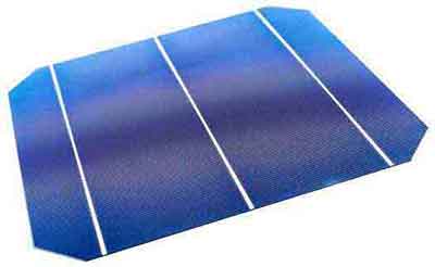
Mono and Poly Solar Cells Available
UniversityWafer supplies mono-crystalline and poly-crystalline solar cells for photovoltaic research and manufacturing applications.
6-Inch Polycrystalline Solar Cells
- 156 × 156 mm dimensions
- 3BB and 4BB configurations
- 17.6–17.8% efficiency
- Higher-efficiency versions above 18%
6-Inch Monocrystalline Solar Cells
- 156 × 156 mm dimensions
- 3BB configuration
- Power output of approximately 4.3 W per cell
- 18.8–19.5% efficiency
5-Inch Monocrystalline Solar Cells
- 125 mm P-type cells
- 2BB design
- 2.8 W output
- SunPower cells with 3.2–3.5 W output
Fast delivery is available for many configurations.
Solar Grade Silicon Wafers
Researchers frequently request solar grade silicon wafers for photovoltaic processing, surface passivation studies, and device characterization. Typical specifications include:
- 100 mm diameter wafers
- <100> orientation
- Boron or phosphorus dopants
- Czochralski (CZ) and Float Zone (FZ) growth methods
- Resistivities from 1–5 Ω-cm
- 280 µm thickness
- Double-side polished surfaces
Solar grade wafers are ideal for developing high-efficiency silicon solar cells and evaluating carrier lifetime, passivation layers, and photovoltaic performance.
Monocrystalline vs Polycrystalline Solar Cells
Monocrystalline silicon cells are fabricated from a single crystal and generally offer higher efficiencies and improved performance. Polycrystalline cells are produced from multiple crystal grains and provide a lower-cost alternative for large-scale solar installations.
| Feature |
Monocrystalline |
Polycrystalline |
| Efficiency |
18–22% |
15–18% |
| Cost |
Higher |
Lower |
| Performance |
Excellent |
Good |
| Applications |
High-efficiency systems |
Large-area installations |
Do Solar Cell Manufacturers Recycle Silicon Kerf?
During wafer slicing, valuable silicon is lost in the form of fine particles called kerf. Recycling silicon kerf has become increasingly important because it helps reduce material costs and improves sustainability in solar manufacturing.
Advanced recovery processes allow manufacturers to reclaim silicon from kerf waste and reuse it in future production cycles. As environmental regulations and material costs continue to rise, kerf recycling is becoming a key component of next-generation photovoltaic manufacturing.
Applications of Silicon Solar Wafers
- Photovoltaic research
- Thin-film solar cells
- High-efficiency solar panels
- Surface passivation studies
- Carrier lifetime measurements
- Multi-junction solar cells
- Concentrator photovoltaics
- Renewable energy development
Related Pages
