H-K9L Glass Wafers Measuremets
A mechanical engineer requested the following quote:
We would like to purchase 20X 2 mm thick rectangular 45 mm x 22 mm pieces of H9KL glass. Please give us a quote and lead time for this.
TTV is different from Peak to Valley (PV) Flatness measurements of a Glass Surface. Do you have a spec for PV Flatness of the glass surface?
Answer:
We do not use PV value to define the flatness of such wafers,
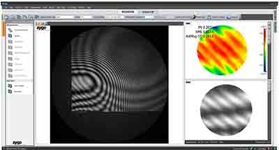
of cause we can measure this value, like as follows by our Zygo machine. So, for such such small chips(45*22mm), the PV should be less than 1λ. Click for image.
Reference #277417 for specs and pricing.
H-K9L with Laser Quality Surface Finish
A optical researcher requested the highest quality glass for their research:
All wafer substrates must be Plano/Plano with parallelism better than 1 arc min and Laser Quality.
8pcs. H-K9L 150mm diameter x 1.5mm thk.
urface Finish: 10/5 Scratch/Dig on both sides.
Surface Flatness, both sides: lambda/8@632.8nm
Thickness tolerance: +/- 0.1mm
Lateral dimension tolerance: +0.0mm/-0.15mm
Reference #225209 for specs and pricing.
Get Your Quote FAST! Or, Buy Online and Start Researching Today!
H-K9L High Refractive Index and Density
When developing optics that are used in extreme environments, it is important to recognize that the optical glass will have a high refractive index and high density of glass, such as the H-K9L. With a lens with this diameter, the densities of the glass become crucial for weight-sensitive applications and help determine the weight of an optical assembly. [Sources: 0]
H-K9L is an excellent less expensive alternative BK7 glass.
H-K9L is a great subsitute for fused silica when extremely hard glass is not required. H-K9L benefits includes:
- low refractive index
- low dispersion
- excellent transmittance through-out the visible and near infrared spectra
Please let us know what specs we can quote for you!
In applications with extreme temperatures and rapid temperature differences, the expansion coefficient of the glass becomes a key factor. The requirements of optical systems for different applications are covered by so many factors that they cannot be met with just a small number of types of glass. Edmund Optics (r) offers a list of eyewear types that can be selected based on the following properties. [Sources: 0]
Spherical aberrations are less present because light travels faster in materials with a lower refractive index. High-index refractions bend light so there is less need for curvature of the lens. [Sources: 0]
Geometric and colored induced aberrations can be compensated by using a wide-angle lens with a high refractive index, such as the H-K9L. [Sources: 0]
Designers typically use the refractive index (Abbe number) of the glass as a degree of freedom when designing systems. The refractive index is a measure of how light interacts with the specified material and slows down when it passes through the optical material. [Sources: 0]
This is determined by the Abbe number (v / d), which is defined as where F / C d is. + 1 (F - C). The x-axis is in the opposite direction, with the number on the left increasing (the number of increases). Fig. 50, and the line starts from bottom to top (starting with number 55) and continues from top to top (Fig. 1). [Sources: 0]
Many glass manufacturers offer the same material properties under different trade names, but most modify the products and processes to be ECO-friendly (lead and arsenic-free), and most of them are "ECO-friendly" or "lead-free" (arsenic-free). The lead letters in the glass names indicate the important chemical elements used in each type of glass. There are large lines that separate different types of glass, such as lead, arsenic, lead - free and free - lead. The deviation is due to the different chemical composition of the different types of glass and their chemical properties. [Sources: 0]
The Abbe diagram, first introduced by SCHOTT in 1923, is a long-established survey of the refractive index of optical glass (d). It indicates the difference between the optical properties of different types of glass in terms of their refractory properties. [Sources: 0]
Zygo Results of H-K9L Glass

What are H-K9L Wafers?
H-K9L, which stands for High-Throughput Leaf Laser, is one of the most popular lasers used today. It is an instrumentation design that utilizes a pulsed beam of laser light for various applications. The laser light is utilized to excite wafers of silicon dioxide (VI) in a semiconductor device. Silicon is the key material that is used to make the lenses and also other parts of the H-K9L. In many ways, this device is considered as a miniature laser printer.
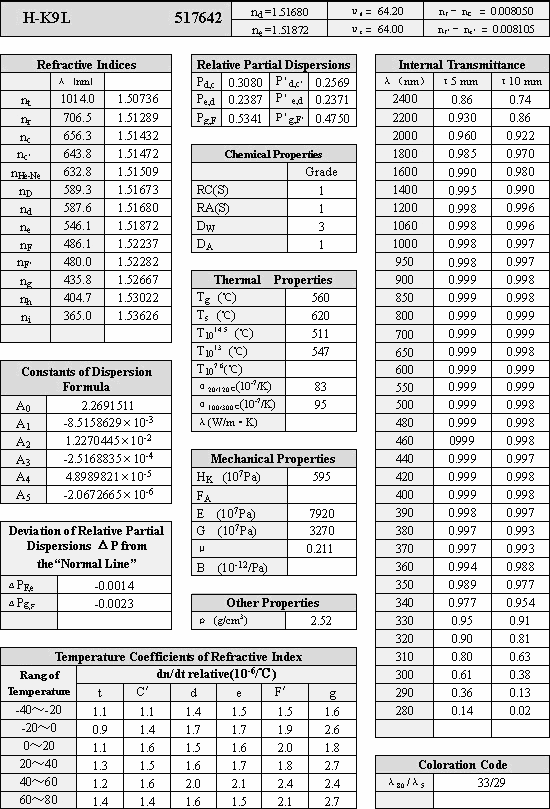
See bottom of this page for H-K9L properties.
A great number of companies manufacture H-K9L optics for a wide range of scientific, medical, industrial, and manufacturing applications.
These devices are highly versatile due to their adaptability to a variety of different application environments. They can be used to scan medical images and thermal imagers.
One application environment includes that of microdissection. Microdissection uses an optical microscope to illuminate tissue samples, such as microphthalmoles, with laser light. The microdissection device consists of a pair of optical lenses. The first lens is typically made from a high index material such as silicon dioxide. The second lens structure is constructed from low index material such as polycarbonate and is attached to the microdissection machine.
Another application environment for H-K9L is that of epitaxial deposition. This method of depositing epitaxial layers results in wafer thickness. Wafer thicknesses are generally in the range of one micrometer or less. In the epitaxial deposition process, a wafer is imprinted with monotonic waves. These waves are formed by passing laser light through the wafer.
Silicon oxide is one of the most common materials used in H-K9L lens structures. Silicon is known for its ability to reflect light. As a result, the silicon dioxide layers can be used to increase lens clarity. Silicon oxide is typically mixed with boron, nitrogen or oxygen. The various combination of materials to create the desirable optical properties.
During microdissection, fine fibers along the edges of the wafer encourage fluid movement. This allows the technician to clearly see into the microdissection sample. The tissue samples can then be stained with different chemicals in order to reveal the contents of the cells. Some microdissection methods rely on injecting special chemicals into the tissues in order to fluorescently label the cells.
Another technique used for studying microdissection samples is the use of optical fibers. These fibers are used to help transmit images down the optical fiber cable. Other uses of microdissection include determining the chemical makeup of a cell, which may help to prevent rejection of an H-K9L lens structure by tissue surgeons. Additionally, this method can be used to study the growth and development of tissues, such as collagen in response to mechanical and biological stimuli. This information is essential to the development of new lenses for therapeutic and prosthetic application.
Microdissection produces a number of scientific findings, many of which are applicable to the field of prosthetics design. For example, studies have shown that epithelial cells are responsible for the smoothness and color of a tissue structure. Specifically, epithelial cell function and recruitment depend on the type of tissue and the depth of microdissection. As such, it is possible to use the findings of microdissection to gain a deeper understanding of how prosthetic lenses are formed and repaired.
Microdissection has also yielded some interesting medical implications. Among these is the use of the technique to detect eye disorders before lenses are placed in the eye. This is particularly important in cases such as macular degeneration, which leads to blindness if treatment is not sought early enough. Additionally, it has been shown that microdissection can be used to detect retinal tear, which is an extremely common problem that leads to many vision problems.
As the success rate of tissue engineering techniques improves, researchers are looking forward to developing microdissection equipment that will allow for greater research success. However, for the time being, the most popular use of this technology is in basic research. As such, there are currently a number of projects using tissue culture microorganisms to grow artificial eyes, among other things. Some of these efforts are being funded by the military, while others are at academic medical centers.
The next step for H-K9L and other tissue engineering applications in this field is to start making tissue products for clinical trials. The goal here would be to find methods of improving vision without increasing visual disturbance. Currently, the only solution to this problem is contact lenses. Other researchers are hopeful of finding better solutions to this problem within the next decade. Until then, keep an eye on the frontiers of this exciting field of research!
H-K9L are the Chinese equivalent of BK7 glass wafers. The specs are nearly the same, but the price for H-K9L windows is much more affordable for researchers and industry.
Please send us your specs and quantity for an immediate quote.
Below are just some of the H-K9L specs that we carry.
Diam 25.4mm, 1000 um thick, DSP
Flatness: better than 1 lambda
---------
Dia 100mm, 1,000 um thick, DSP
TTV < 1um
Roughness <1nm
Parallelism <1 arcsec
---------
H-K9L Glass Wafers
150mm 675um
DSP
60/40
---------
H-K9L
20x20x1.0mm, DSP
---------
H-K9L is a type of glass used to make wafers for use in microelectromechanical systems (MEMS) and other microelectronic devices. H-K9L is a borosilicate glass that has a low coefficient of thermal expansion, which means that it expands very little when heated. This property makes it ideal for use in MEMS devices, which often experience temperature changes during operation.
H-K9L wafers are typically made using a process called flame hydrolysis deposition, in which borosilicate glass is deposited onto a substrate using a flame. The resulting wafers are characterized by their high purity, good surface finish, and excellent mechanical and chemical stability.
H-K9L wafers are used in a variety of applications, including the production of microfluidic devices, sensors, and actuators. They are also used as a substrate for the growth of thin films and as a material for the fabrication of microelectronic devices. In addition to these applications, H-K9L wafers are also used in research and development for a variety of other applications.
H-K9L Materials Property

H-K9l Datasheet

