Electrical-Grade Germanium for MBE
A senior process development engineer requested a quote for the following.
We need a quote for the following.
4 piece of Ge Wafer (100) 2" dia x 0.5 mm, DSP, P type ( Ga doped), resistivities: 0.1-0.5ohm-cm, and
4 piece of Ge Wafer (100) Undoped, 2" dia x 0.5 mm, resistivities: >50 ohm-cm, DSP
We would use these for MBE growths. What is the difference between the ones you quoted versus the epi ready ones (Ge 001 double side polished, both doped and undoped), both in terms of surface preparation and pricing?
Reference #250149 for specs and pricing.
Get Your FAST! Or, Buy Online and Start Researching Today!
Electrical Grade Germanium (Ge) Wafers
Germanium wafer applications can divided into five categories.
Germanium is also used to fabricate electronic devices such as transistors when doped with g - germanium (G).
We have a large selection of Electrical and Optical Grade Germanium Single and double side polished wafers in stock and ready to ship.

What are Some Germanium Wafer Facts?
A Germanium wafer is also known as a Germanium substrate, a wafer substrate or a photovoltaic wafer. The Germanium used in the manufacturing of solar cells is the reason why a Germanium wafer can be used to make the thin film which is used to make solar cells for residential homes. The Germanium used for this process is actually an inexpensive metal that has a large influence on how the wafer will conduct electricity. Another reason the use of the material is very economical is because it can be used in a wide variety of applications.
The Germanium wafer is made from a mixture of phosphors and sulfur in a quartz structure. This structure results in a very thin, transparent film. There are two different grades used to make the wafer. The first grade is what is called the optical grade used to make the solar cell conductor, the second grade is the electrical grade used to make the solar cell. The germanium crystals used are a perfect conductor for electricity and as a result the wafer is able to conduct electricity very well.
The high refractive index of the germanium wafer makes it a perfect conductor for electricity because the energy absorbed by the light cannot escape to the interior of the wafer. As a result the light is very bright and there are very low losses with this type of wafer. The reason the electrical conductivity is so high with these materials is because the conductivity of most other materials would be very low, but germanium wafers have a high refractive index due to the materials used.
Many people are not aware of the unique properties of this material. The germanium wafer has been used in the manufacturing of some of the better night vision goggles because of the amazing light transmission. You may not have noticed it before, but if you look at some night-vision goggles from past years you will notice that the night vision was brighter and had much more focus than other night vision goggles. These germanium wafers have a special coating on the surface that allows them to have a focus that other wafers do not have. Due to the unique properties of the Germanium wafer it is being used in more electronics.

Electrical Grade Germanium Is a Valuable Metal For a Variety of Applications
When manufacturing solar cells, electrical grade Germanium is an ideal material to use as the conductor. This material is very good at conducting electricity, and is doped with g-germanium (G). It can be easily cut into thin sheets, resulting in a transparent film. It is also very durable, making it an excellent choice for semiconductor devices. This type of semiconductor can be used in a variety of applications, from batteries to semiconductor devices and transistors.
Electrical grade Germanium is typically a wafer or a substrate. It is used in the manufacturing of solar cells. It is also a good choice for making thin film for residential solar cells. This metal is inexpensive and has a large impact on the conductivity of a wafer. As a result, it is a great choice for solar cells and a wide variety of other applications. It is available in a variety of grades and has a high conductivity.
Germanium is an inexpensive metal that can be found in many different applications. In addition to solar cells, it can also be used in a variety of other electronics. For instance, it can be incorporated into a solar cell thin film for residential use. The Germanium used in this process is a cheap metal, and has a significant influence on the conductivity of the wafer. Due to its low price, it is a popular choice for solar cell manufacture.
Electrical grade Germanium is also a valuable metal for a variety of other applications. It can be a useful material in solar cells. It can be used to create a thin film for residential solar cells. Its low price makes it very economical to use. It has a broad range of applications, ranging from the manufacturing of solar cells to many other industrial uses. However, it can also be used in a variety of other ways, including making thin films for electrical wiring.
This type of solar cell is also known as a Germanium substrate, or a Germanium wafer. It is used in the manufacturing of solar cells. It can be used to make a thin film for residential solar cells. This type of semiconductor is an economical material, and can be used in a variety of applications. It can also be used in the manufacturing of thin films for other products. Using this material is an excellent choice for making a solar cell.
In addition to solar cells, Germanium is used as a substrate for solar cells. It is a popular material for the manufacturing of thin film solar cells. It is also used in the manufacturing of solar cell components. This material can be used in both residential and commercial solar cells. This inexpensive metal is used in many different applications. Its low price makes it an excellent choice for a wide variety of other products. It is also a great choice for manufacturing a thin film for residential solar cells.
Germanium wafers can be used to make residential solar cells. This material is also used in the production of thin-film solar cells. The cost of this material makes it a good choice for a wide range of applications. A Germanium wafer is a highly versatile and economical material. It can be used in a wide variety of applications. While it is an inexpensive and versatile metal, it has limited applications. Its use in the solar industry is limited.
Germanium wafers are another popular material. These wafers are a relatively inexpensive material that is used for solar cells. They can be used to manufacture thin-film residential solar cells and can be used as a substrate for photovoltaics. It is also used to make the thin-film solar cells that are so popular in commercial and residential solar cells. Because it is a cheap metal, it is an attractive option for a wide variety of applications.
Its conductivity is incredibly high. It is widely used in solar cells and can be used to create solar cells. It is also used in thin-film solar cells and is used in a variety of other applications. It is also a great choice for making home batteries. And its low cost makes it a viable option for any application. This type of semiconductor material can be a good choice for many reasons. The cost is very low, and there are no specialized processes involved.
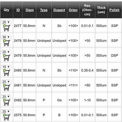
Electrical Grade Ge Wafers Inventory
P-type Gallium Doped Germanium Substrates
- Ge Substrate (111) 5 x 5 x 0.5 mm, SSP, P-type ,Ga-doped ,R: 0.005-0.01 ohm.cm
- Ge Substrate: (100) 5x5 x 0.5 mm , SSP, P type Ga doped,R:0.0007-0.002 ohm.cm
- Ge Substrate: (100) 5x5 x 0.5 mm , SSP, P type Ga doped,R:1-5 ohm.cm -1
- Ge Substrate: (100) 10x5 x 0.5 mm , SSP, P type Ga doped,R:1-5 ohm.cm
- Ge Substrate: (100) 10x5 x 0.5 mm , DSP, P type Ga doped,R:0.1-0.5 ohm.cm
- Ge Substrate (110)+/- 0.7 degree 5x5x0.5 mm, SSP,Sb-doped ,R:0.1-0.5 ohm.cm
- Ge Substrate (110) 10x5x 0.5 mm, SSP, Sb-doped ,R:0.1-0.5 ohm.cm
- Ge Wafer (110) Ga-doped, 2" dia x 0.5 mm, SSP Resistivity : 0.1-0.5 ohm-cm
- Ge Wafer (110) Ga-doped, 2" dia x 0.5 mm, SSP Resistivity : 1-10 ohm-cm
- Ge Wafer (110) Ga-doped, 2" dia x 0.5 mm, DSP Resistivity : 0.1-0.5 ohm-cm
- Ge Wafer (110) Ga-doped, 2" dia x 0.5 mm, DSP Resistivity : 1-5 ohm-cm
- Ge Substrate: (100) 10x10 x 0.5 mm , DSP, P type Ga doped,R:0.1-0.5 ohm.cm
- Ge Substrate: (100) 10x10 x 0.5 mm , DSP, P type Ga doped,R:1-5 ohm.cm-1
- Ge Wafer (100) 2" dia x 0.5 mm, SSP, P type ( Ga doped), resistivities: 1-10 ohm-cm
- Ge Wafer (100) 2" dia x 0.5 mm, SSP, P type ( Ga doped), resistivities: 0.1-0.5ohm-cm
- Ge Wafer (100) 2" dia x 0.5 mm, SSP, P type ( Ga doped), resistivity: 0.001-0.005 ohm-cm
- Ge Wafer (100) 2" dia x 0.5 mm, SSP, P type ( Ga doped), resistivity: 0.005-0.009 ohm-cm
- Ge Wafer (100) 2" dia x 0.5 mm, SSP, P type ( Ga doped), resistivity: 0.01-0.1 ohm-cm
- Ge Wafer (100) 2" dia x 0.5 mm, DSP, P type ( Ga doped), resistivities: 0.1-0.5ohm-cm
- Ge Wafer (100) 2" dia x 0.5 mm, DSP, P type ( Ga doped), resistivities: 0.14-0.23 ohm-cm
- Ge Wafer (100) 2" dia x 0.5 mm, DSP, P type ( Ga doped), resistivities: 0.23-0.24ohm-cm
- Ge Wafer (100) 2" dia x 0.5 mm, DSP, P type ( Ga doped), resistivities: 1 - 10 ohm-cm
- Ge Wafer (100) 2" dia x 0.5 mm, DSP, P type ( Ga doped), resistivity: 0.001-0.005 ohm-cm
- Ge Wafer (100)+/- 2 degree , 2" dia x 0.5 mm, DSP, P type ( Ga doped), resistivities: 10-15 ohm-cm
- Ge Wafer (111) 2" dia x 0.4 mm, DSP, P type ( Ga doped) Resistivities: 0.035-0.039ohm-cm
- Ge Wafer (111) 2" dia x 0.5 mm, SSP, P type ( Ga doped), Resistivities: 0.022-0.026 ohm-cm
- Ge Wafer (111) 2" dia x 0.5 mm, SSP, P type ( Ga doped), resistivities: 10-20 ohm-cm
- Ge Wafer (111) 2" dia x 0.5 mm, SSP, P type ( Ga doped), resistivities: 1-10 ohm-cm
- Ge Wafer (111) 2" dia x 0.5 mm, SSP, P type ( Ga doped), resistivities:0.005-0.01 ohm.cm
- Ge Wafer (111) 2" dia x 0.5 mm, DSP, P type ( Ga doped) resistivities: 0.005-0.01ohm-cm
- Ge Wafer (111) 2" dia x 0.5 mm, DSP, P type ( Ga doped) resistivities: 0.007-0.008ohm-cm
- Ge Substrate: (100) 10x10 x 0.5 mm , SSP, P type Ga doped,R:0.0007-0.002ohm.cm-1
- Ge Substrate: (100) 10x10 x 0.5 mm , SSP, P type Ga doped,R:0.001-0.005 ohm.cm
- Ge Substrate: (100) 10x10 x 0.5 mm , SSP, P type Ga doped,R:1-5 ohm.cm
- Ge Wafer (100) 2" dia x 0.4 mm, DSP, P type ( Ga doped), resistivities: 0.1ohm-cm
- Ge Substrate (111) 10x10x 0.5 mm, SSP, P-type ,Ga-doped ,R: 0.005-0.01 ohm.cm
- Ge Substrate: (100)+/- 2 degree, 10x10 x 0.5 mm , DSP, P type Ga doped,R:10-15 ohm.cm
N-type Antimony Doped Germanium Substrates
- Ge Wafer (100) 2" dia x 0.5 mm, SSP, N type ( Sb doped), resistivity:2.5-2.7ohm-cm
- Ge Substrate (111) 10x5x 0.5 mm, DSP, Sb-doped . 0.005-0.01 Ohm.cm
- Ge Wafer (110)N type, Sb doped, 2" dia x 0.5 mm, SSP Resistivity: 0.82-0.98ohm.cm
- Ge Wafer (110)N type, Sb doped, 2" dia x 0.5 mm, SSP Resistivity: 1-5ohm.cm
- Ge Wafer (110)N type, Sb doped, 2" dia x 0.5 mm, DSP Resistivity: 0.1-0.5ohm.cm
- Ge Wafer (110)N type, Sb doped, 2" dia x 0.5 mm, DSP Resistivity: 1-5ohm.cm
- Ge Substrate: (100) 10x10 x 0.5 mm , SSP, N type Sb doped,R:0.1-0.5 Ohm.cm
- Ge Substrate: (100) 10x10 x 0.5 mm , SSP, N type Sb doped,R:10-15Ohm.cm
- Ge Substrate: (100) 10x10 x 0.5 mm , SSP, N type Sb doped,R>40 Ohm.cm
- Ge Wafer (111) 2" dia x 0.5 mm, SSP, N type ( Sb doped), resistivities: 0.005-0.01ohm-cm
- Ge Wafer (111) 2" dia x 0.5 mm, SSP, N type ( Sb doped), resistivities: 0.01-0.1ohm-cm
- Ge Wafer (111) 2" dia x 0.5 mm, SSP, N type ( Sb doped), resistivities: 0.05-0.5ohm-cm
- Ge Wafer (111) 2" dia x 0..5 mm, DSP, N type ( Sb doped), R: 0.005-0.01 ohm-cm-1
- Ge Wafer (111) 2" dia x 0..5 mm, DSP, N type ( Sb doped), R: 0.007-0.009 ohm-cm
- Ge Wafer (111) 2" dia x 0.5 mm, DSP, N type ( Sb doped), R: 10.5-15.2 ohm-cm
- Ge Wafer (111) 2" dia x 0.5 mm, DSP, N type ( Sb doped), resistivities: 0.2-0.26 ohm-cm
- Ge Wafer (100) 2" dia x 0.5 mm, DSP, N type ( Sb doped), Resistivities: 1-5 ohm-cm
- Ge Wafer (100) 2" dia x 0.5 mm, DSP, N type ( Sb doped), R:>40 ohm-cm
- Ge Wafer (100) 2" dia x 0.5 mm, DSP, N type ( Sb doped), resistivities: 0.01-0.1 ohm-cm
- Ge Wafer (100) 2" dia x 0.5 mm, DSP, N type ( Sb doped), resistivities: 10-20 ohm-cm
- Ge Wafer (100) +/- 1 degree, 2" dia x 0.5 mm, DSP, N type ( Sb doped), resistivities: 0.1-0.5 ohm-cm
- Ge Substrate (110) 10x10x 0.5 mm, SSP, Sb-doped ,R:1-5 ohm.cm
- Ge Substrate (110)+/- 0.7 degree 10x10x 0.5 mm, SSP, Sb-doped ,R:0.1-0.5 ohm.cm
- Ge Wafer (111) with 9.45 degree miscut , 2" dia x 0.5 mm, SSP, N type ( Sb doped), resistivities: 0.1-0.5ohm-cm
- Ge Wafer (100) +/- 2 degree , 2" dia x 0.5 mm, SSP, N type ( Sb doped), R:0.1-0.5 ohm.cm
- Ge Wafer (100) +/- 3 degree , 2" dia x 0.5 mm, SSP, N type ( Sb doped), R:0.1-0.5 ohm.cm
- Ge Wafer (100) +/- 4 degree , 2" dia x 0.5 mm, SSP, N type ( Sb doped), R:0.1-0.5 ohm.cm
- Ge Wafer (100) 2" dia x 0.5 mm, SSP, N type ( Sb doped), R:>40 ohm-cm
- Ge Wafer (100) 2" dia x 0.5 mm, SSP, N type ( Sb doped), resistivities:0.01-0.1 ohm-cm
- Ge Wafer (100) 2" dia x 0.5 mm, SSP, N type ( Sb doped), resistivities:10-15 ohm-cm
- Ge Wafer (100) 2" dia x 0.5 mm, SSP, N type ( Sb doped), resistivities:1-5 ohm-cm
- Ge Wafer (100) with 3 degree miscut , 2" dia x 0.5 mm, SSP, N type ( Sb doped), R:0.27-0.35 ohm.cm
- Ge Wafer (100) 2" dia x 0.5 mm, SSP, N type ( Sb doped), Resistivities: 0.001-0.01 ohm-cm
- Ge Substrate (111) 10x10x 0.5 mm, DSP, Sb-doped . 0.005-0.01 Ohm.cm
- Ge Substrate (111) 10x10x 0.5 mm, DSP, Sb-doped . 0.005-0.01 Ohm.cm
- Ge Substrate: (100) 10x10 x 0.5 mm , DSP, N type Sb doped,R:0.01-0.1 Ohm.cm -1
- Ge Substrate: (100) 5x5 x 0.5 mm , SSP, N type Sb doped,R:0.1-0.5 Ohm.cm
- Ge Substrate: (100) 5x5 x 0.5 mm , SSP, N type Sb doped,R>40 Ohm.cm
Undoped Germanium Substrates
- Ge Wafer (100) Undoped, 2" dia x 0.45 mm, SSP, resistivities: >50 ohm-cm
- Ge Wafer (100) Undoped, 2" dia x 0.5 mm, SSP, resistivities: >50 ohm-cm
- Ge Wafer (100) Undoped, 2" dia x 0.5 mm, resistivities: >50 ohm-cm, DSP
- Ge Substrate (111) 5x5x 0.5 mm, DSP, Undoped
- Ge Substrate (110) 5x5x 0.5 mm, SSP, Undoped
- Ge Substrate (110) 10x5x 0.5 mm, SSP, Undoped
- Ge Substrate (110) 10x5x 0.5 mm, DSP, Undoped
- Ge Wafer Undoped, 1" dia x 0.5 mm, SSP (100) R:>45 Ohm.cm
- Ge Substrate (100) 5x 5x0.5 mm, DSP, Undoped
- Ge Wafer . Undoped, 2" dia x 0.5 mm, SSP (111) R >50 ohm.cm
- Ge Wafer . Undoped, 2" dia x 0.5 mm, DSP (111) R >50 Ohm.cm
- Ge Wafer (110) Undoped, 2" dia x 0.5 mm, SSP, R:>50 ohm.cm
- Ge Wafer (110) Undoped, 2" dia x 0.5 mm, DSP,R:>50 ohm.cm
- Ge Wafer (100) Undoped, 1" dia x 0.5 mm, DSP,R:>50 ohm.cm - GEUa25D05C2
- Ge Wafer (110) Undoped, 1" dia x 0.5 mm, SSP,R:>50 ohm.cm
- Ge Wafer (111) Undoped, 1" dia x 0.5 mm, SSP, R:>50 ohm.cm
- Ge Wafer (111) Undoped, 1" dia x 0.5 mm ,DSP, R:>50 ohm.cm
- Ge Wafer Undoped (100) 3" dia x 0.5 mm SSP resistivity: >50 ohm-cm
- Ge Wafer Undoped (100) 3" dia x 0.5 mm DSP resistivity: >50 ohm-cm
- Ge Wafer Undoped (110) 3" dia x 0.5 mm SSP resistivity: >50 ohm-cm
- Ge Wafer Undoped (110) 3" dia x 0.5 mm DSP resistivity: >50 ohm-cm
- Ge Substrate (100) 10x10x 0.35 mm, SSP, Undoped
- Ge Substrate (100) 10x10x 0.45 mm, SSP, Undoped
- Ge Substrate (100) 10x10x 0.5 mm, SSP, Undoped
- Ge Substrate (100) 10x10x 0.5 mm, DSP, Undoped
- Ge Substrate (110) 10x10x 0.5 mm, SSP, Undoped, R>50 ohm.cm5
- Ge Substrate (110) 10x10x 0.5 mm, DSP, Undoped
- Ge Substrate (111) 10x10x 0.45 mm, DSP, Undoped
- Ge Substrate (111) 10x10x 0.5 mm, SSP, Undoped
- Ge Substrate (111) 10x10x 0.5 mm, DSP, Undoped
- GOI -Ge layer with <100> with 10 degrees towards the (111) on Insulator wafer,6" dia


