What is Silicon Epitaxy?
Silicon epitaxy is a process in which a layer of material is grown on top of a substrate. In the case of silicon epitaxy, this would involve growing a layer of silicon on top of a substrate material. This is typically done in the production of semiconductor devices, such as transistors, where it is important to have a precisely controlled layer of silicon with specific properties. Silicon epitaxy can be achieved using a variety of techniques, such as chemical vapor deposition or molecular beam epitaxy.
What is NPN Silicon Epitaxial Transistor?
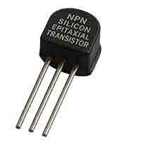
A silicon epitaxial transistor is a type of transistor that is made using silicon epitaxy. In this process,
 a layer of silicon is grown on top of a substrate material, typically using chemical vapor deposition or molecular beam epitaxy. The resulting layer of silicon has specific properties that are necessary for the proper operation of a transistor.
Epitaxial Silicon Density
The density of epitaxial silicon refers to the amount of silicon atoms per unit volume in an epitaxially grown layer of silicon. This value can vary depending on the specific growth conditions used, such as the temperature and pressure of the growth process, as well as the type of substrate material used. In general, the density of epitaxial silicon is higher than the density of bulk silicon, which is typically around 2.33 grams per cubic centimeter. The density of epitaxial silicon can range from around 2.4 to 2.6 grams per cubic centimeter, depending on the growth conditions.
Silicon Epitaxy Method
There are several methods that can be used to achieve silicon epitaxy, including chemical vapor deposition (CVD) and molecular beam epitaxy (MBE).
- In chemical vapor deposition (CVD), a silicon-containing gas is introduced into a growth chamber, where it is decomposed and deposited onto a heated substrate material. This method allows for the precise control of the growth process, and it can be used to produce high-quality epitaxial layers of silicon.
- Molecular beam epitaxy (MBE) is a similar process, in which silicon atoms are evaporated and directed onto a substrate material using a focused beam of particles. This method allows for the growth of extremely thin layers of silicon with precise control over the layer thickness and cWomposition.
What is Silicon Epitaxy Rate?
The rate at which silicon epitaxy occurs refers to the speed at which the epitaxial layer of silicon grows during the growth process. This rate can be affected by a variety of factors, such as the type of growth technique used, the temperature and pressure of the growth process, and the type of substrate material. In general, the silicon epitaxy rate will be higher at higher temperatures and lower pressures, and it can range from around 1 to 10 micrometers per minute, depending on the specific growth conditions.
What is Silicon Epitaxial Planar Transistor
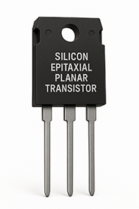
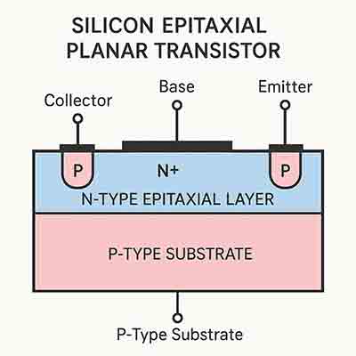
A silicon epitaxial planar transistor is a type of transistor that is made using a process called silicon  epitaxy, in which a layer of silicon is grown on top of a substrate material. This type of transistor is called a "planar" transistor because the layers of the transistor are flat and uniform, as opposed to other types of transistors where the layers are non-uniform or "non-planar". A silicon epitaxial planar transistor is typically used in high-performance applications, such as in computer microprocessors, because of its superior electrical properties compared to other types of transistors.

Silicon Epitaxial Planar Transistor Cross-Section Diagram"
Epitaxial Silicon Wafer Production
To produce epitaxial silicon wafers, a layer of silicon is grown on top of a substrate material using a process called silicon epitaxy. This is typically done using chemical vapor deposition (CVD) or molecular beam epitaxy (MBE), in which a silicon-containing gas is introduced into a growth chamber and deposited onto a heated substrate material. The resulting epitaxial layer of silicon has specific properties that are necessary for the proper operation of semiconductor devices. The wafers are then cut from the epitaxial layer and polished to produce smooth, high-quality surfaces.
Silicon Epitaxy Process
Basics
Silicon epitaxy is a process used for semiconductor fabrication. It can be used to create a single crystal silicon film that is uniformly deposited on a silicon  substrate. The method involves several simultaneous chemical reactions that result in the growth of a semiconductor crystal layer. It is particularly useful for compound semiconductors. It offers a high crystalline quality, which is essential for highly complex microprocessors. In addition, it offers improved doping control and electrical properties.
The use of epitaxy to improve the electrical characteristics of a bare silicon wafer is a significant advantage. It can also help to perfect the crystal structure of a bare silicon wafer. In addition, it can provide a layer that is free of bulk defects. For example, it can be used to grow a thin layer of crystalline silicon over a sapphire substrate.
Other applications of epitaxy include strain engineering techniques. In these techniques, tensile and compressive strains are created in the channel of a transistor. In the semiconductor industry, this technique is employed to generate super junction structures that are required for power MOSFETs that require higher voltages. In these devices, the channel is close to the surface of the wafer, which conducts loads efficiently towards metal contacts. However, there are some drawbacks. For instance, there are issues with the amount of defect formation in the channel.
In addition, it can be difficult to implement III-V and Ge on a silicon wafer. Despite these issues, epitaxy is becoming increasingly important for the semiconductor industry. For example, it has played a large role in chip designs, especially in the channels. Among other things, it can boost hole mobility. Additionally, it can create a pn junction that is close to the surface, which helps to conduct loads efficiently. In bipolar devices, it can prevent latchup, which is an issue for CMOS circuits.
The main limitations to epitaxy are its limited processing capabilities. For example, current electron-beam lithography cannot produce well-defined 30-nm pitch patterns. Moreover, it cannot produce large area patterns. Another limitation is the deposition tool's throughput. Other manufacturing concerns are the cleanliness and cleanliness of the chamber atmosphere, as well as the prevention of diffusion of dopant atoms on the wafer's surface.
A growing area of interest in the epitaxy field is molecular-beam epitaxy, or MBE. In MBE, a semiconductor film is grown from melt on a solid substrate. The film's lattice must be aligned with the crystalline lattice of the substrate. In this case, the growth rate of the epitaxial film depends on the mole fraction of reactants. The epitaxial layer can be a single crystal, or it can be made to form a double-crystalline layer. The process can be modified to suit specific requirements.
The new etch patterns for silicon are designed to reduce the time of epitaxial deposition by as much as 40%, and to significantly reduce the number of defects. The etch variations shown in these figures are at two depths, which are corresponding to the first and second stages of the deposition/etching cycle.
Characteristics of epitaxial films
Silicon epitaxy is a process where multiple layers of semiconductor materials are grown on the same substrate. It is widely used in the semiconductor industry. Although this process is complicated, it has several advantages. In particular, it can be used to grow polycrystalline material.
The process involves several simultaneous chemical reactions. Each step requires a specific chemical compound or gas to be applied. For example, the first step involves melting a thin layer of silicon onto the substrate. It is then cooled slowly to form the layer. This enables the atoms to move freely on the surface of the substrate. The layer is then patterned to form a variety of shapes. The final product is a highly stable device.
The rate of growth of the epitaxial layer depends on the mole fraction of reactants and the temperature of the solid. It also depends on the crystal orientation of the substrate. However, it is also affected by external factors. A higher growth rate indicates that the crystals are being grown in the proper position. If the epitaxial film is not properly grown, it can result in strain buildup on the substrate.
For this reason, it is important to understand the physics behind the process. This allows researchers to develop accurate models for the epitaxial growth of crystals. In addition, this will allow them to make better decisions about the optimal growth conditions.
During the early stages of epitaxy, the process requires modeling of the surface chemistry and overgrowth kinetics. This will help researchers determine whether the material will be able to resist or resorb the byproducts of the chemical reaction. This is especially important when a high quality device is being manufactured. It is necessary to control the growth process to ensure that a device will be stable and function appropriately.
There are two main types of silicon epitaxy. The first is called homoepitaxy. This means that the epitaxial layer is made from the same compound as the substrate. The other type is heteroepitaxy, which means that the material is formed from a different compound.
In order to produce epitaxial films with a certain optical property, scientists use a combination of x-ray diffraction, reflection high energy electron diffraction, and spectroscopic ellipsometry. These techniques provide scientists with information about the thickness and optical properties of the epitaxial layer.
The growth of the epitaxial film is a complex process. In the initial stages, the film's lattice is aligned with the crystalline lattice of the substrate. This is done by tilting the epitaxial layer. Then, a layer of a different material is placed on top of the epitaxial layer. This enables the atomic layer to be measured using a wavelength of light. Eventually, the crystalline structure is deposited on the silicon wafer.
The growth of thin silicon epitaxial layer is a very complex process. It requires the use of nitrogen and hydrogen gases. It also involves the dissolving of the silicon layer on the wafer. The results are a thin layer of silicon with a good resistivity.
Process control
When designing and constructing silicon-based devices, epitaxy plays an important role. It is a process that forms crystalline thin films on substrates. These layers are used in electronic and optoelectronic applications. However, the fabrication of epitaxial structures from thermally decomposed materials is challenging. Therefore, process control is essential.
The growth rate of epitaxial layers depends on a number of factors. The chemical sources involved in the epitaxial process, as well as the crystal orientation of the substrate, are important determinants. The rate of growth can also be affected by external factors. The rate of cooling can also affect the quality of the film. In addition, epitaxial layers can be of different electrical properties.
The epitaxial film is formed by a series of chemical reactions that occur simultaneously. These reactions are controlled using a variety of methods. One method is evaporation. Another involves a high-temperature chamber. In the latter case, a gas such as nitrogen or hydrogen is used to form a thin layer on the substrate.
The rate of epitaxial growth is not fixed and can be controlled by using different combinations of impurities and dopants. For example, some of the most common materials used in epitaxial growth are oxides, gallium arsenide, and boron doped silicon. In addition to these materials, other substrates can be utilized for specific applications.
The first step in the process is to partially dissolve a silicon layer on the substrate. Then, a silicon epitaxial film is formed. This layer can be manufactured in a single layer or in a multi-layer format. The epitaxial growth rate is also a significant factor in the stability of the device.
The next step in the epitaxial process is to deposit a thin layer of a different material over the epitaxial film. This is done in order to provide a source for electrons and control the conductivity of the channel. This is called heteroepitaxy.
The most common type of epitaxial layer is the p-type. It is characterized by high-quality silicon, and is widely used in the semiconductor industry. It is also a good candidate for solar cell applications. It has also been successfully incorporated in various other devices, including CMOS transistors, memory devices, and optoelectronics.
There are several kinds of epitaxial structures. They can be classified according to the type of growth method. In this article, we will discuss two types of CVD systems used for epitaxial growth. The advantages and disadvantages of each system will be discussed.
In the early stages of epitaxy, the nucleation and overgrowth kinetics of the process need to be modeled. The modeling must link nucleation and overgrowth kinetics to surface chemistry and reconstruction. These models can be used for process optimization and troubleshooting. In addition, these models can be applied to design and optimize the next generation of CVD chambers.
Epitaxy is an exciting field of research. In the future, it will play an important role in computing and communications.
Molecular Beam Epitaxy Silicon Wafer
A molecular beam epitaxy (MBE) silicon wafer is a type of wafer that is made using the molecular beam epitaxy (MBE) growth process. In this process, a beam of silicon atoms is directed onto a heated substrate material, where they deposit and form a layer of silicon. This method allows for the growth of extremely thin layers of silicon with precise control over the layer thickness and composition. The resulting MBE silicon wafer has high-quality electrical and optical properties that make it suitable for use in a variety of applications, such as in the production of semiconductor devices and solar cells.
