
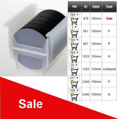
⚡ In Stock Ready to Ship Silicon Wafers
Below is just an example of what we have in stock. We also have P-Type, N-Type of all dopants and specs. Buy as few as one wafer!
100mm Undoped Silicon
(100) Orientation, >20,000 ohm-cm, SSP, 500µm Thickness.
We have 1,000 wafers of this spec available immediately.
Get Your Silicon Wafer Quote FAST! Or, Buy Online and Start Researching Today!
Why Buy From Us?
- No Minimums: Buy 1 wafer or 1,000.
- Global Sourcing: We source from top manufacturers like SUMCO to ensure semiconductor-grade quality.
- University Friendly: We accept Purchase Orders from all major universities.
Shop Silicon Wafers by Diameter
Select a size below to view real-time inventory and pricing.

How to Choose the Right Silicon Wafer Spec
Choosing the correct wafer specification is critical for yield and device performance. Below are the key parameters to consider.
1. Wafer Grade
- Prime Grade: The highest quality, meeting strict SEMI standards for TTV (Total Thickness Variation), Bow, and Warp. Used for photolithography and device fabrication.
- Test Grade: Similar to Prime but with slightly looser flatness specs. Ideal for equipment testing, thin film deposition, and process monitoring.
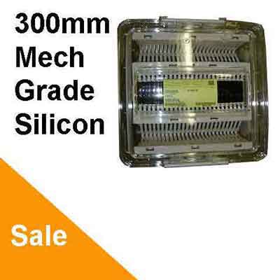
- Mechanical/Dummy Grade: The most economical option. May have minor surface defects. Used for handling practice, mechanical calibration, and non-critical thermal testing.
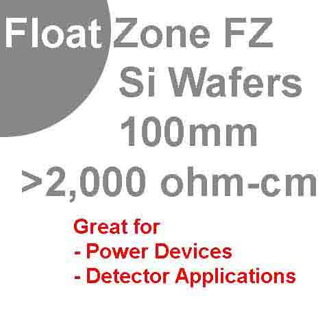
2. Crystal Growth Method: CZ vs. FZ
Czochralski (CZ): The most common method. Silicon is pulled from a molten crucible. It contains interstitial oxygen which improves mechanical strength and provides internal gettering sites for impurities.
Float Zone (FZ): Grown without a crucible, resulting in extremely high purity and low oxygen content. FZ wafers are required for high-efficiency solar cells and high-voltage power devices.
3. Crystallographic Orientation
The orientation of the silicon lattice affects etch rates and electrical properties.
- <100>: The most common orientation. Preferred for MOSFETs and general CMOS applications due to lower interface trap density.
- <111>: Has the highest atomic packing density. It oxidizes faster and has the highest thermal expansion coefficient (~5 ppm/°C). It is often used for bipolar devices.
4. Thermal Expansion Coefficients
For applications involving high heat (up to 400°C), understanding thermal expansion is vital. The <111> direction expands the most (~5 ppm/°C), while the <100> direction expands the least (~2.6 ppm/°C).
Common Applications
- Microfluidics: 100mm and 150mm wafers are often used as substrates for etching micro-channels.
- Optics: Silicon is transparent to infrared light, making polished wafers excellent for IR lenses and windows.
- Calibration: We supply wafers with specific thicknesses (e.g., 1.5mm or 2mm) for calibrating dicing saws and wafer handling robots.
- Nanotube Growth: Silicon wafers serve as the stable substrate for carbon nanotube fabrication.
Need to recycle your old wafers?
Silicon wafers can be recycled! The process involves breaking down wafers and purifying the silicon for reuse in solar or other industries. Contact us if you have surplus inventory.