
I was looking for Fe (iron) doped Silicon wafers. I checked the website but not able to find them. Can you please help me out if you have Iron coated silicon wafers? Can I get the quote for 2 iron coated wafers? I am also looking for Patterned substrates with Cu and Si stripe dimensions of ~160 micrometre and ~60 micrometres.
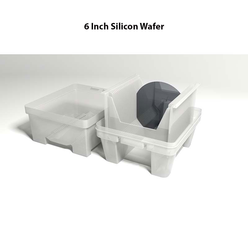
Large Selection of 6 Inch Silicon Wafers In stock
You can buy as few as one wafer or large volumes. We cater to researchers needing high-quality but affordable substrate for their experiments. The price of silicon wafers is based on specs and quantity.
Researcher:
Please reference #255361 for specs and pricing.
Get Your 6 Inch Silicon Wafer Quote FAST! Or, buy online and start researching today!
Below Are Just Some of the 6 Inch Silicon Wafers that We Carry
We have a large selection of standard and hard to find specs in stock. We work with the researcher to provide the best specs for their research.
Wafer Dopings:
- Undoped, Boron (B), Gallium (Ga), Arsenic (As), Antimony (Sb), Degenerately Doped
Wafer Types
Wafer Oris
- (100), (111), (110), (112), (531), (510), (311), (211)
What is The Cost of 6 Inch (150mm) Silicon Wafers
Taiwan-based manufacturers are reporting soaring demand for 6 Inch Silicon Wafers. The rise in demand for 5G, AI, and cloud computing is driving a small increase in production costs. Plessey LEDs have undergone a final process to develop a patented technology, available in production quantities. In 2019, FBK fabricated three-dimensional pixels on six-inch silicon wafers using 150-mm-thick SOI wafers.
China is the largest consumer of 6 Inch Silicon Wafers, with demand expected to increase seven-fold over the next decade. The growth of 4G and future technologies will drive future wafer prices.
6 Inch Silicon Substrated Used for Spin Coating Optical Adhesives
A government researcher requested: "SSP... using these wafers for spincoating optical adhesives, the other specs (type, dopant) aren't that important to us".
- Diameter: 6", Doping: Any, Ori: (100), Resistivity: >100 ohm-cm, Thickness: 1000um, Quantity: 25
Reference #194619 for specs and pricing.
Where Can You Buy 6 Inch Silicon Wafers Online?
Here are just some of the ongoing sales. Swipe left/right on mobile to see all columns.
| Item | Type/dop | Orient. | Diam. | Thck (μm) | Pol | Resistivity Ohm-cm |
|---|---|---|---|---|---|---|
| TS006 | P/B | [100] | 6" | 525 ±15 | P/E | MCZ 0.01--0.02 |
| SEMI Prime, 1 SEMI Flat 57.5mm @ <011>±0.5°, Oxygen=(11--13)ppma | ||||||
| TS004 | P/B | [100] | 6" | 675 ±15 | P/E | MCZ 0.01--0.02 |
| SEMI Prime, 1 SEMI Flat 57.5mm @ <011>±0.5°, Oxygen=(3--9)ppma | ||||||
| TS005 | P/B | [100] | 6" | 675 ±15 | P/E | MCZ 0.01--0.02 |
| SEMI Prime, 1Flat 57.5mm @ <001>±0.5° | ||||||
| K667 | P/B | [100] | 6" | 900 | C/C | FZ >1,000 |
| SEMI Prime, 1Flat (57.5mm), Empak cst | ||||||
| 7038 | P/B | [111] ±0.5° | 6" | 875 | P/E | FZ >10,000 |
| SEMI Prime, 1Flat (57.5mm), Empak cst | ||||||
| 6898 | P/B | [111] ±0.5° | 6" | 1,000 | P/E | FZ >5,000 |
| SEMI Prime, 1Flat (57.5mm), Empak cst | ||||||
| 7208 | N/Ph | [100] ±1° | 6" | 1,000 ±50 | P/P | FZ >9,500 |
| SEMI Prime, 1Flat (57.5mm), Empak cst, Lifetime>6,000μs | ||||||
| E239 | N/Ph | [100] | 6" | 825 | C/C | FZ 7,000--8,000 |
| SEMI, 1Flat, Lifetime=7,562μs, in Open Empak cst | ||||||
| F907 | N/Ph | [100] | 6" | 3,000 | P/P | FZ >4,800 |
| SEMI Prime, 1Flat (57.5mm), Individual cst, Lifetime>7,000μs | ||||||
| 7212 | N/Ph | [100] ±1° | 6" | 450 | P/P | FZ 4,300--8,300 |
| SEMI Prime, 1Flat (57.5mm), Empak cst | ||||||
| 7233 | N/Ph | [100] ±1° | 6" | 675 | P/P | FZ 4,300--8,300 |
| SEMI Prime, 1Flat (57.5mm), Empak cst | ||||||
| L625 | N/Ph | [100--6°] | 6" | 625 | P/E | FZ >3,500 |
| SEMI Prime, 1Flat (57.5mm), Empak cst | ||||||
| E700 | N/Ph | [100--6°] | 6" | 675 | P/P | FZ >3,500 |
| SEMI Prime, 1Flat (57.5mm), Empak cst | ||||||
| F700 | N/Ph | [100--6°] | 6" | 790 ±10 | C/C | FZ >3,500 |
| SEMI, 1Flat, Empak cst | ||||||
| 4982 | N/Ph | [100--6°] | 6" | 675 | P/P | FZ >1,000 |
| SEMI Prime, Notch on <010>, Laser Mark, Empak cst | ||||||
| D982 | N/Ph | [100--6°] | 6" | 675 | BROKEN | FZ >1,000 |
| SEMI notch Broken, Empak cst | ||||||
| 7122 | N/Ph | [100] | 6" | 500 ±10 | P/P | FZ 50--70 |
| SEMI Prime, 1Flat, Empak cst | ||||||
| G122 | N/Ph | [100] | 6" | 500 ±10 | P/P | FZ 50--70 |
| SEMI Prime, 1Flat, Empak cst | ||||||
| 5325 | N/Ph | [100] | 6" | 725 | P/P | FZ 50--70 |
| SEMI Prime, 1Flat (57.5mm), Lifetime=15,700μs | ||||||
| 7053 | N/Ph | [100] | 6" | 2,000 | P/P | FZ 50--70 |
| SEMI Prime, 1Flat (57.5mm) | ||||||
| 6883 | N/Ph | [100] | 6" | 625 ±5 | P/P | FZ 40--90 |
| SEMI Prime, 1Flat (57.5mm), TTV <3μm | ||||||
| G883 | N/Ph | [100] | 6" | 650 ±5 | P/P | FZ 40--90 |
| SEMI Prime, 1Flat (57.5mm), TTV<3μm | ||||||
| F883 | N/Ph | [100] | 6" | 675 ±5 | P/P | FZ 40--90 |
| SEMI Prime, 1Flat (57.5mm), TTV<3μm | ||||||
| S5622 | N/Ph | [100] | 6" | 1,300 ±10 | E/E | FZ 0.01--0.05 |
| SEMI notch, Empak cst | ||||||
| G228 | N/Ph | [111] ±0.5° | 6" | 300 ±15 | BROKEN | FZ >6,000 |
| Test, Broken into pieces, ranging 65% to 5% | ||||||
| N445 | N/Ph | [112--5.0°] | 6" | 875 ±10 | E/E | FZ >3,000 |
| SEMI, 1Flat (47.5mm), TTV<4μm, Surface Chips | ||||||
| G343 | N/Ph | [112--5°] | 6" | 1,000 ±10 | C/C | FZ >3,000 |
| SEMI, 1 JEIDA Flat (47.5mm), TTV<4μm, Lifetime>1,000μs | ||||||
| 7116 | Intrinsic | [100] | 6" | 675 | P/P | FZ >65,000 |
| SEMI notch Prime, Empak cst | ||||||
| M526 | Intrinsic | [100] ±0.1° | 6" | 720 ±10 | P/P | FZ >10,000 |
| SEMI Prime, 1Flat (57.5mm), TTV<3μm | ||||||
| 7117 | Intrinsic | [111] ±0.5° | 6" | 875 | P/P | FZ >10,000 |
| SEMI Prime, 1Flat (57.5mm), Empak cst | ||||||
| F613 | P/B | [110] ±0.5° | 6" | 300 | P/P | 20--25 |
| SEMI TEST -- scratched, can be repolished, 2Flats | ||||||
| G458 | P/B | [110] ±0.5° | 6" | 390 ±10 | C/C | >10 |
| 2Flats, Empak cst | ||||||
| TS002 | P/B | [110] ±0.25° | 6" | 625 ±15 | P/E | 10--20 |
| SEMI Prime, 1 JEIDA Flat (47.5mm) @ <111>, TTV<3μm, Bow<5μm | ||||||
| TS007 | P/B | [110] ±0.25° | 6" | 625 ±15 | P/E | 10--20 |
| SEMI Prime, 1 JEIDA Flat 47.5mm @ <111>±0.5°, LaserMark, TTV<2μm | ||||||
| TS072 | P/B | [110] ±0.25° | 6" | 625 ±15 | P/E | 10--20 |
| SEMI Prime, 1 JEIDA Flat (47.5mm) @ <111>±0.5°, TTV<3μm | ||||||
| 6427 | P/B | [110] ±0.5° | 6" | 675 | P/E | 0.01--0.02 |
| Prime, PFlat @ [111]±0.25°, SF @ [111]±5° | ||||||
| TS054 | P/B | [100] | 6" | 675 | P/E | 15--25 |
| SEMI Prime, 1Flat (57.5mm), TTV<5μm | ||||||
| 4980 | P/B | [100] | 6" | 220 | P/P | 10--30 |
| SEMI 1Flat, TEST grade (scratches), TTV<4μm | ||||||
| L405 | P/B | [100] | 6" | 1,000 | P/P | 10--15 |
| SEMI Prime, 1Flat, Empak cst | ||||||
| 7066 | P/B | [100] | 6" | 675 | P/P | 5--10 |
| SEMI Prime, 1Flat (57.5mm) | ||||||
| 6287 | P/B | [100] | 6" | 675 | P/E | 5--10 |
| SEMI Prime, 1Flat (57.5mm) | ||||||
| 6751 | P/B | [100] | 6" | 1,000 | P/E | 5--10 |
| SEMI Prime, 1Flat (57.5mm) | ||||||
| 7030 | P/B | [100] | 6" | 1,000 | P/E | 5--10 |
| SEMI Prime, 1Flat (57.5mm) | ||||||
| E964 | P/B | [100] | 6" | 475 | P/P | 1--30 |
| SEMI Prime, 1Flat (57.5mm) | ||||||
| 5964 | P/B | [100] | 6" | 500 | P/P | 1--30 |
| SEMI Prime, 1Flat (57.5mm), TTV<5μm | ||||||
| D964 | P/B | [100] | 6" | 500 | P/P | 1--30 |
| SEMI Prime, 1Flat (57.5mm), TTV<5μm | ||||||
| 5354 | P/B | [100--9.7°] | 6" | 525 | P/P | 1--100 |
| SEMI Prime, 1Flat (57.5mm) at <110>±0.1° | ||||||
| B420 | P/B | [100] | 6" | 675 | P/P | 1--5 |
| SEMI Prime, 1Flat, Soft cst | ||||||
| 6358 | P/B | [100--6°] | 6" | 675 | P/E | 1--30 |
| SEMI Prime, 1Flat (57.5mm) | ||||||
| N698 | P/B | [100] | 6" | 675 | P/E | 1--100 |
| SEMI Prime, 1Flat (57.5mm) | ||||||
| 6404 | P/B | [100] | 6" | 800 | E/E | 1--50 |
| SEMI, 1Flat (57.5mm), TTV<5μm | ||||||
| F162 | P/B | [100] | 6" | 2,000 ±50 | P/P | 1--35 |
| SEMI Prime, 1Flat (57.5mm), Individual cst | ||||||
| E162 | P/B | [100] | 6" | 2,000 ±50 | P/E | 1--35 |
| SEMI Prime, 1Flat (57.5mm), Back-Side polished with small scratches | ||||||
| 7047 | P/B | [100] | 6" | 400 | P/P | 0.5--1.0 |
| SEMI Prime, 1Flat (57.5mm) | ||||||
| S5821 | P/B | [100] | 6" | 275 | P/P | 0.01--0.05 |
| SEMI Prime, 1Flat (57.5mm), TTV<2μm | ||||||
| TS104 | P/B | [100] | 6" | 625 ±15 | P/EOx | 0.01--0.02 |
| SEMI Prime, JEIDA Flat 47.5mm, Back-side LTO | ||||||
| TS055 | P/B | [100] | 6" | 675 ±15 | P/E | 0.01--0.02 |
| SEMI Prime, 1Flat (57.5mm) | ||||||
| TS103 | P/B | [100] | 6" | 525 ±15 | P/E | 0.007--0.015 |
| SEMI Prime, 1Flat (57.5mm), TTV<5μm | ||||||
| 6005 | P/B | [100] | 6" | 320 | P/E | 0.001--0.030 |
| JEIDA Prime, Empak cst | ||||||
| 6484 | P/B | [100] | 6" | 675 | P/E | 0.001--0.005 |
| SEMI Prime, 1Flat (57.5mm) | ||||||
| TS108 | P/B | [111--3°] | 6" | 625 ±15 | P/E | 0.01--0.02 |
| SEMI Prime, 1Flat (57.5mm), TTV<8μm | ||||||
| J668 | P/B | [111] ±0.5° | 6" | 675 | E/E | 0.010--0.025 |
| SEMI, 1Flat (57.5mm), TTV<5μm | ||||||
| TS105 | N/As | [111--1.5°] | 6" | 675 | P/EOx | 0.001--0.002 |
| SEMI Prime, 1Flat, Back-side LTO, TTV<6μm | ||||||
| 5814 | N/Ph | [100] | 6" | 925 ±15 | E/E | 5--35 |
| JEIDA Prime, TTV<5μm | ||||||
| B728 | N/Ph | [100] | 6" | 675 | P/E | 2.7--4.0 |
| SEMI Prime, Empak cst | ||||||
| TS063 | N/Ph | [100] | 6" | 525 | P/E | 1--3 |
| SEMI Prime, 1Flat (57.5mm) | ||||||
| TS075 | N/Ph | [100] | 6" | 525 | P/E | 1--3 |
| SEMI Prime, Flat: JEIDA 47.5mm, Oxygen=(10--14)ppma | ||||||
| TS076 | N/Ph | [100] | 6" | 525 | P/E | 1--3 |
| SEMI Prime, Flat: JEIDA 47.5mm, Oxygen=(10--14)ppma | ||||||
| 6971 | N/Ph | [100--25°] | 6" | 675 | P/P | 1--100 |
| SEMI notch Prime, TTV<1μm | ||||||
| 6965 | N/Ph | [100] | 6" | 675 ±10 | P/E | 1--10 |
| SEMI Prime, 1Flat (57.5mm) | ||||||
| 7170 | N/Ph | [100] ±1° | 6" | 675 | P/E | 1--20 |
| Prime, 2 SEMI Flats, Back-side Acid etched | ||||||
| C716 | N/Ph | [100--28°] | 6" | 700 | P/P | 1--100 |
| SEMI Notch Prime, TTV<2μm | ||||||
| S5913 | N/Ph | [100] ±1° | 6" | 800 | P/E | 1--10 |
| SEMI Prime, 1Flat (57.5mm) | ||||||
| F859 | N/Ph | [100--25°] | 6" | 800 | C/C | 1--100 |
| SEMI notch Prime, Empak cst | ||||||
| E089 | N/Ph | [100] | 6" | 1,910 ±10 | P/P | 1--100 |
| SEMI Prime, 1Flat (57.5mm), TTV<2μm | ||||||
| F089 | N/Ph | [100] | 6" | 1,910 ±10 | P/P | 1--100 |
| SEMI Prime, 1Flat (57.5mm), TTV<5μm | ||||||
| G844 | N/Ph | [100] | 6" | 5,000 | P/P | 1--35 |
| SEMI Prime, 1Flat (57.5mm), Individual cst | ||||||
| L066 | N/Sb | [100] | 6" | 675 | P/E | 0.01--0.02 |
| SEMI Prime, 1Flat (57.5mm) | ||||||
| C673 | N/Sb | [100] | 6" | 675 | P/E | 0.008--0.020 |
| SEMI Prime, 1Flat (57.5mm) | ||||||
| 2533 | N/As | [100] | 6" | 1,000 | L/L | 0.0033--0.0037 |
| SEMI, 1Flat(57.5mm), in individual wafer cassettes | ||||||
| E533 | N/As | [100] | 6" | 1,000 | L/L | 0.0033--0.0037 |
| SEMI, 1Flat(57.5mm) | ||||||
| TS018 | N/As | [100] | 6" | 575 ±15 | P/P | 0.001--0.005 |
| SEMI Prime, 2Flats (PF @ <110>), Laser Mark | ||||||
| 4204 | N/As | [100] | 6" | 675 | P/EOx | 0.001--0.005 |
| SEMI Prime, 1Flat, Back-side LTO, TTV<4μm | ||||||
| 5541 | N/Ph | [100] | 6" | 675 | P/EOx | 0.001--0.002 |
| SEMI Prime, 1Flat, with strippable Epi layer | ||||||
| TS101 | N/As | [100] | 6" | 675 ±15 | P/EOx | 0.001--0.005 |
| SEMI Prime, 1Flat (57.5mm), TTV<5μm, LTO | ||||||
| TS037 | N/Ph | [111--1.5°] | 6" | 675 | P/E | 3--12 |
| SEMI Prime, 1Flat (57.5mm) | ||||||
| 6559 | N/Ph | [111] ±0.5° | 6" | 675 | P/E | 1--100 |
| Prime, NO Flats, Empak cst | ||||||
| TS112 | N/As | [111--4°] | 6" | 508 | P/E | 0.0038--0.0042 |
| SEMI Prime, 1Flat (57.5mm), Back-side LTO | ||||||
| TS034 | N/As | [111--4°] | 6" | 625 ±15 | P/EOx | 0.0024--0.0035 |
| SEMI Prime, 1Flat, Back-side LTO | ||||||
| TS109 | N/As | [111--4°] | 6" | 508 ±15 | P/E | 0.0023--0.0026 |
| SEMI Prime, 1Flat (57.5mm), TTV<8μm | ||||||
| TS102 | N/As | [111--4°] | 6" | 675 | P/E | 0.001--0.005 |
| SEMI Prime, 1Flat, TTV<4μm, Bow<10μm, Warp<20μm | ||||||
| TS107 | N/As | [111--2.5°] | 6" | 625 ±15 | P/EOx | 0.001--0.004 |
| SEMI Prime, JEIDA Flat (47.5mm), Back-side LTO | ||||||
How to Make the Most of 6 Inch Silicon Wafers
Several manufacturers have begun developing six-inch and eight-inch wafers. While larger silicon wafers are cheaper to produce, they aren't yet mainstream and can be of lower quality than four-inch counterparts. Choosing the right orientation will maximize the efficiency of semiconductor production. It is important to identify the type of silicon wafer needed; the best wafers are mirror-like and have uniform surfaces.
During manufacturing, it is important to select the proper orientation to help maximize efficiency. Making 6 inch silicon wafers is highly efficient, allowing for more precision and uniformity in the final product. A six-inch silicon wafer is more expensive than a one-inch wafer but allows for more flexibility during machining.