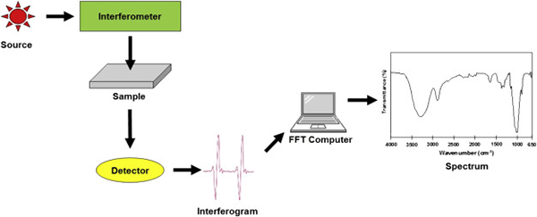
Fourier-Transform Infrared Spectroscopy (FTIR)
Fourier-Transform Infrared Spectroscopy (FTIR) Undoped Silicon
Below is one of our silicon items that is great for FTIR Spectroscopy.
Si Item #3193
100mm Undoped <100> >10,000 ohm-cm 525um DSP Prime
Silicon shows promise to be the next-evolution anode material for lithium-ion batteries (LIBs). But Silicon electrodes exhibit significant capacity fade with cycling.
Researchers theorizes that the capacity loss is due to the solid electrolyte interphase (SEI) forming in the first cycle and becoming destabilized by large cyclic volume changes.
A client researcher used our item 3193 for the following cell for in situ attenuated total reflection-Fourier transform infrared spectroscopy with controllable penetration depth was used to study the chemistry at the electrode–electrolyte interface.
Get Your Undoped Silicon Wafer for (FTIR) Quote FAST!
FTIR Spectroscopy
What is Fourier Transform Infrared Spectroscopy?
3D printing with Jobin and Yvon Horiba is described here, and the material includes Raman microscopes and more. [Sources: 2]
We evaluated the effect of the sensor's performance and properties using linear spectroscopy, using a high-resolution spectrometer (MS) and a spectrograph (IR - MS spectral data) to evaluate the content of active ingredients, auxiliary agents and uniformity. We searched the IR and MS spectral data with a specially designed solid phase FTIR library that contained a wide range of spectral properties such as absorption, spectral resolution and sensitivity, as well as the presence of drug additives and excitants in the spectral spectrum. This has proven to be an imaging and chemical subceptometry sensitivity of up to 1.5 micrometres per millimetre, which is about 1,000 times higher than the current standard of 1 mm per micrometre. [Sources: 2, 3, 5]
The GC - FTIR data acquisition and processing was performed with a high-resolution spectrometer (MS) and a spectrograph (IR - MS spectral data) with high resolution. [Sources: 5]
The spectrometer board should also be attached to a cube (3D printed here) and the module contains a laser and Raman spectroscopy interface optics, which allows high-quality ramen spectra to be recorded from the sample. A typical nano-FTIR setup consists of two components: a broadband infrared light source used for peak illumination and a Michelson interferometer that acts as a Fourier transformation spectrometer. The light is excited by a flexible optical fiber through Raman spectroopy. This light can be emitted via a micrometer-sized fiber optic cable or a fiber optic cable. [Sources: 1, 2]
By measuring the small energy differences due to the spectral signature of the probe - the sample coupling between the sample and the Fourier transformation spectrometer - FTIR spectroscopy enables the problem of differentiating between regioisomer compounds in the presence of an energy-rich light source such as a fiber optic cable to be overcome. This allows the detection of spectral signatures produced by the probes - samples that are coupled to each other and allow the identification of compounds with a variety of properties, which can lead to the development of new applications in materials science and engineering, as well as chemical and biological applications. [Sources: 1, 3, 5]
The complementary use of FTIR and Raman spectroscopy can also be used to thoroughly investigate processes that occur in the sol-gel process. There are a number of applications where the detection of coherent anti-Stokes and Raman scattering can contribute to the identification of regioisomer compounds and their properties. Several candidates based on optical spectrography have been discussed, such as Fourier optical transformation spectrometry and infrared FTIR spectroopy, but there is no clear consensus on whether the combination of two different spectra types - FTIR and optics - can be supported in the discovery of a new class of compounds with different properties in a variety of materials. [Sources: 1, 2, 6]
Raman spectroscopy is often used in chemistry to obtain a structural fingerprint that can identify molecules. It is named after Raman, one of the founders of chemical engineering and a pioneer in the field of chemistry, and it was used to characterize and identify the chemical composition and structure of unknown materials. [Sources: 2]
FTIR spectroscopy is a dispersion method, meaning that measurements can be made in a variety of places, such as the surface of a thin-film sample. In other words, nano-FTIR has the ability to restore the same information as ellipsometry or impedance spectrography, which typically provide the same information from thin-film samples, but with a further spatial resolution in the nanoscale range. This allows the chemical composition and structure of thin films to be measured much more accurately and their chemical properties to be directly compared and reported, as well as processed in real time and to provide information about their properties and properties. [Sources: 1, 2, 4]
When the microphone signal is plotted as a function of the wavelength, it contains a spectrum proportional to the absorption spectrum of the sample, and the corresponding absorption spectrum is obtained. The second term in the above equation is not dependent on the reference mirror position and only contributes the direct current signal for the Fourier transformation. Another advantage of FTIR spectroscopy is that it is semi-continuous, so interferograms can typically be obtained in less than five seconds. [Sources: 1, 4, 6]
Photoluminescence and Raman spectra of porous silicon testify to silicon nanocrystallites remaining in pores with great optical penetration depth. Most medicines have a high concentration of silica, which is evident from the fact that a large number of molecules present in the form of a single molecule (e.g. a drug molecule) interact with the silica structure, which leads to a rotational imetry of the molecule that confirms the rearrangement of chemical groups. The changes in porous silicon size (Si) can be investigated by observing ramen scattering and by spectroscopy. [Sources: 0, 6]
Combine rheology and Raman spectroscopy for analysis and learn more about IR spectroscopy in our interactive tutorial here. The process and analysis technology, including a 3D-printed cylindrical tablet made of the acrylic polymer Eudragit L100 - 55, is evaluated by loading paracetamol with a high concentration of Silicon nanocrystallites (Si) in the form of a single molecule (e.g. a drug molecule) into it and evaluating the spectra with the help of an infrared spectrometer (IR spectrograph). The processes and analytical technologies, which include a 4-D laser, a 2-dimensional electron microscope and an optical spectroscope, are evaluated by using Par-Acetate - a robust 3D printable cylINDrical tablet made of an acrylic polymer (EadragitL100-55) in a ratio of 1: 1 silica to silicon. [Sources: 2]
Sources:
[0]: https://www.hindawi.com/journals/isrn/2011/163168/
[1]: https://en.wikipedia.org/wiki/Nano-FTIR
[2]: https://letsboost.net/87xb/3d-printed-raman-spectrometer.html
[3]: https://www.pnas.org/content/111/20/7191
[4]: https://www.sciencedirect.com/topics/engineering/fourier-transform-infrared-spectrometer
[5]: https://www.frontiersin.org/articles/10.3389/fchem.2020.00624/full
[6]: https://www.intechopen.com/books/applications-of-molecular-spectroscopy-to-current-research-in-the-chemical-and-biological-sciences/fourier-transform-infrared-and-raman-characterization-of-silica-based-materials
Wafers Used for Fourier Transform Infrared Measurements?
Many people are familiar with the wafers used in microwave cooking. These pieces of plastic are coated or made to look like an aluminum foil and are placed in a microwave oven. They produce an infrared signal as heat passes over them. Wafers have been used for many different applications throughout the history of science, especially in the areas of physics, astronomy and electronics. The foil has also been used for optical measurements.
As a tool for the scientific and technology communities, wafers are used for many different purposes. They can be made to be flat or curved. They can have different thicknesses, widths and heights.
There is a wide range of other uses for them in science and technology research too. One application that is becoming popular is for the creation of a substrate for the FET or Field-effect Transistor. A substrate is a non-volatile semiconductor material that allows electrical currents to pass through it.
The wafers are used for many different kinds of experiments. In electronics, they are often used as a substrate for the fastener regions of circuits. This material is thin, but has great conductivity. It is a semiconductor material and so can be used for many different kinds of experiments.
A variety of industries use wafers for infrared measurement. In electronics they are used to detect the presence of impurity in semiconductors. This can tell an engineer if there is a defect, something that could lead to catastrophic failures in the design of a chip. They are also used in many manufacturing processes to aid in the detection of moisture, which could lead to problems with the machines.
Engineers also use wafers for many other purposes. Some use them for the purpose of measuring temperatures inside of objects. These are known as thermal wafers and can be found for things such as refrigeration lines, industrial ovens and some kinds of medical equipment. Many medical applications for wafers have been developed over the years and you will often find that they are very thin, making them ideal for doing these measurements.
There are many different kinds of wafers, some which are used for both F-number measurement and for infrared detection. The F-number shows the frequency of the infrared signal. By measuring the frequency of the signal, you can determine the temperature of the substance being measured.
There are many different kinds of wafers available. Some are made of metallic materials, others are made from plastic and still others are made from ceramic. All of these wafers will work and provide the accurate results that you are looking for. When you look for a wafer, you should keep several things in mind. For one thing, you need to look for ones that are made from the best possible material, as this is a very important measurement.
When you begin to look for wafers for F-number measurement, it is a good idea to look for ones which have a high F-number. In fact, the higher the number, the better the result. In addition to this, wafers which are low in density are also a good choice for infrared measurement. One of the most popular types of wafers for this measurement is called Spheres. These come in a variety of shapes, but they are also made of many different materials so you should have no problem finding some that suit your needs.
When looking for wafers for F-number measurement, it is a good idea to look for ones that are coated with an inert gas. If you use ordinary wafers, then they may produce infrared signals, which will not work very well. In order to ensure that your measurements are all taken from the same waveform, then you should also consider using waveguides. These allow you to easily pinpoint the exact location of a transmitter by taking the infrared signal and measuring it against another waveform.
Another option that many people use for F-number measurement is a tabletop scale. These are great if you do not want to place too heavy or expensive equipment on your workbench, as they are much easier to handle. There are even some wafers which are made to fit on a standard workbench. These work particularly well if there is not enough room around the wafer to place another device.
You can also buy wafers online. This can be a convenient way of finding the perfect wafer for your needs, and you may also save money by buying in bulk. Many websites will sell their products at lower prices than you would find in most local stores. Although some may be slightly higher in price, you will always get a high quality wafer that will work perfectly. You will also be able to order these wafers online, which will save you time and money and will reduce the risk of getting your wafers damaged during shipping.
What is the Difference Between FTIR & Raman?
Both Fourier Transform Infrared Measurements and Raman spectroscopy are spectroscopy techniques. The respective spectroscopy techniques capture rich spectra of many different substrates like silicon and other materials.
Here are each spectroscopy benefits:
- FTIR is an excellent choice for manufacturing applications such as quality control, failure analysis, and process development
- RAMAN is a superior choice for chemical analyses and 3-D depth profiling of optically transparent substances.
Each of these chemometrics technologies are also widely used in the field of plastics identification and characterization. In fact, these two spectroscopic techniques are the two most common methods for plastics identification and characterization. Moreover, both are useful in identifying microplastics in the environment, the accumulation of microplastics in biological specimens, and the oxidation of polymers in consumer goods.
FTIR uses the Fourier Transform Infrared (FTIR) spectroscopy, while Raman measures energy scattered by photons from a sample. FTIR is based on the fact that a light source will scatter a particular molecule, whereas the Raman method measures the energy scattered by the sample. This technique is favored by researchers because it is non-invasive and non-destructive, and can detect pathological conditions and biominerals.
FTIR and Raman are complementary spectroscopy techniques that are used for identifying and fingerprinting molecules. Unlike FTIR, Raman spectroscopy has many advantages over FTIR and IR spectroscopy. The difference between FTIR and RAMAN is so subtle that it is not worth discussing in this article. You can use a combination of these methods in a scientific paper or patent application.
FTIR is implemented as a single-purpose instrument. IR is used in chemical research. In addition to being non-destructive, FTIR can be combined with other spectroscopy techniques to provide high-resolution chemical analyses. FTIR can be miniaturized into handheld devices. Similarly, Raman spectroscopy can be done on any material. However, FTIR is more sensitive to polarization than Raman.
FTIR is more sensitive than Raman, but FTIR has greater resolution. Using a FTIR spectroscopy, the FTIR spectrum shows the chemical purity of a sample, while a Raman spectroscopy can reveal the structural distribution of a chemical. If both FTIR and IR are used together, they can give very high-resolution information about a material.