
I need two silicon carbide substrates, double side polished, 25.4mm diameter, as thick as possible. Please include shipping cost with quote.
Silicon Carbide (SiC) Substrates 4H and 6H Epi-Ready
We have a surplus high-quality, low cost test grade 100mm 4H Silcon Carbide wafers. Please contact us for specs and pricing.
100mm 4H Silicon Carbide Substrate Sale!
It can be hard to find a good supplier of silicon carbide wafers that meets your needs. We have a large selection of Silicon Carbide wafers in stock. From small diced pieces to larger diameters. Below is an example of how we help researchers in academia and industry:
Researcher Request:
Reference #214215 for specs and pricing.
4H N-Type Silicon Carbide Substrates
Postdoc Request:
Could you give me some pricing for in stock 4" diameter 4H n-
type silicon carbide wafers? These are for reactive ion etch process development so no other critical specifications.
Reference #221899 for specs and pricing.
Get Your Quote FAST! Or, Buy Online and Start Researching Today!
Silicon Carbide Wafer Suppliers
Not all silicon carbide wafers are created equal. You need a supplier that has a large selection of different sizes and thicknesses to meet your specific needs.
UniversityWafer, Inc. is the perfect supplier for you. We have a large selection of silicon carbide wafers in both 4h and 6h of different grades and in thicknesses and diameters you need. Plus, we offer the best prices in the industry.
Silicon Carbide (SiC) wafer benefits are better than Silicon and Gallium Arsenide. SiC properties work great for the following applications:
- Short wavelength opto-electronic
- High-temperature
- Radiation resistant
- High-power/high-frequency electronic devices
You can buy as few as one wafer in diameters ranging from 5mm x 5mm up to 150mm.
Many are in stock and ready to ship.
Our Silicon Carbide (SiC) wafers are used to fabricate High-Powerd Devices
Watch https://www.youtube.com/embed/_ttNDQTkvHc
Silicon Carbide (SiC) Semiconductor Market - By Device
- Discrete Device
- Diode
- MOSFET
- Module
- Bare Die
Silicon Carbide Semiconductor Market - By Vertical
- Telecommunications
- Energy & Power
- Renewable Energy & Photovoltaic
- Automotive
- EV
- HEV
- Military & Defense
I need 15-30 mm thickness and 4 to 8 inch diameter wafer, it should be clear and no pipes inside. Like crystal clear and full white in color.
White Silicon Carbide Ingot for Moissanite Diamond
This super white SiC crystal is using for Moissanite Diamond,"clear and no pipes inside. Like crystal clear and full white in color".

Watch https://www.youtube.com/embed/U0DmrzQT4cY
Please ask for pricing.
Silicon Carbide (SiC) Thin Films
Let us know how we can help you!
SiC thin films were grown onto polished p-type Si (100) wafers. Good crystallinity in the thin layers is desirable, as it affects different material properties. Since the sIC thin film deposits in amorphous nanocrystalline structures at low temperatures, a post-treatment such as annealing is necessary to improve the crystallination of the material.
Research shows that the ionized state is in the range of 0.5 - 1.1% of the total area, depending on the separation parameters and target composition. This seems to be very attractive, as it produces stuttering atoms and thus facilitates the formation of a crystalline phase. These properties allow the deposition of thin layers of nanocrystalline structures at low temperatures and the formation of thin layers with high - or low - pressure. Although there are no known techniques, the crystallinity of SICs differs considerably in the methods used, but low-pressure plasma-based techniques have been studied to enable deposition at room temperature, such as plasma-enhanced chemical dapor deposition and plasmionization.
Further details on the HiPIMS reactor are elsewhere, but the target is maintained at 3 mTorr, which is a flow rate of 20 sccm. The thin film is applied to an Aln buffer, which is equipped with a high-temperature, low-pressure and high-volume reactor (HV).
The carrier holder is held at a cutting time and a target value - the distance between the carrier material is set to 60 min or 60 mm, and 200 or 400 w are embedded for film growth. The floating potential of the film increases to 1.5 mTorr, with a float rate of 20 sccm and a floating potential ratio of 2.0.
Silicon Carbide Wafer Specs to Fabricate Power Devices
A scientist requested a quote for SiC wafers:
We need to practice etching and do not have other specs yet, but should mimic power devices. Can you recommend and quote? Can you thin 500um SiC wafers down to 350um?
UniversityWafer Replied and Quoted:
Power devices do not use 500um thick wafers; for 100mm products, a thickness of 350um is used. Will this meet your
No Integrated Device Mfg (IDM) wants to back-grind this 500um wafer down to a thinner level for device performance (On Resistance). 350um is the standard thickness that meets the need for shape control in the fab and thin enough to minimize the back-grinding process at the end of line.
Please ask for the specs and quote. Reference #254927.
4H Silicon Carbide (SiC) Wafers for Tunneling Microscopy
Researchers have used the following silicon carbide specs for their tunneling microscopy experiments.
2" SiC 4H-N, Research grade SSP with higher conductivity
Silicon Carbide for Epitaxial Research
Researcher:
I am looking for both C-face and Si-face epi-ready 2inch diameter 4H-SiC wafer with 4 deg off-axis. I need n+doped and insulating from each. Also, I would like to inquire about 100 mm wafer price as a possible option for my work. These would be standard grade SiC wafers.
UniversityWafer, Inc. Quoted:
Price depends on quantity.
- both C-face and Si-face epi-ready 2inch diameter 4H-SiC wafer with 4 deg off-axis. n+doped,thickness 0.3-0.5 mm,as epitaxial substrate for growths
- both C-face and Si-face epi-ready 2inch diameter 4H-SiC wafer with 0 deg off-axis. insulating,thickness 0.3-0.5 mm,as epitaxial substrate for growths
- both C-face and Si-face epi-ready 4inch diameter 4H-SiC wafer with 4 deg off-axis. n+doped,thickness 0.3-0.5 mm,as epitaxial substrate for growths
- both C-face and Si-face epi-ready 4inch diameter 4H-SiC wafer with 0 deg off-axis. insulating,thickness 0.3-0.5 mm,as epitaxial substrate for growths
Why are Silicon Carbide (SiC) Better than Sapphire and Glass for Bonding with Silicon?
A PHD student asked the following:
Actually, I know that sapphire and glass wafers can be used as carrier wafers, but I am wondering why SiC are used as carriers. What are they bonded to?
UniversityWafer, Inc. Replied:
SiC are used as carriers due to the good flatness and good thermal conductivity. SiC is better than sapphire and glass, as the silicon can bonded onto the SiC much more easily!
To learn more reference 262947.
4H Silicon Carbide Wafer Sale
We have a sale on the following silicon carbide substrate. We can dice the wafer into any dimension. Please let us know if you can use, or if you need another SiC spec or a quote for another substrate. Please forward to your fellow researchers you think could use.
We have the following in stock! Buy as few as one for very low price!
Crystal Characteristics
Poly-type: 4H
Doping Type: N-Type
Dopant: Nitrogen
Surface Orientation degrees: 3.8-4.2
Wafer Mechanical Characteristics
Diameter: 100mm
Thickness Microns: 325-375um
Primary flat position degrees: +/-1
Primary flat length (mm): 30.5-34.5
Secondary flat position (mm): +/-05
Secondary flat length (mm): 16-20
Substrate Quality
Resistivity: 0.010-0.030
Foreign Polytypes: <15
Off-Axis from 11-20: 4
Spec sheet available upon request.
What are Semi-Insulating Silicon Carbide Substrate
Semi-Insulating Silicon Carbide (SiC) Substrate Overview
Semi-insulating Silicon Carbide (SiC) substrates are specialized materials used for high-power, high-frequency, and radiation-resistant electronic applications. Unlike conductive SiC, semi-insulating SiC has high resistivity (10⁶ – 10⁹ Ω·cm), making it ideal for devices requiring electrical isolation and thermal stability.
Key Properties of Semi-Insulating SiC
- Wide Bandgap (3.26 eV for 4H-SiC): Enables operation at high voltages and temperatures.
- High Thermal Conductivity (~4.9 W/cm·K): Efficient heat dissipation for power electronics.
- High Breakdown Electric Field (~3.2 MV/cm): Supports high-voltage operations.
- Radiation Hardness: Resistant to harsh environments, making it suitable for aerospace and defense.
Applications of Semi-Insulating SiC Substrates
1. RF & Microwave Devices
- High Electron Mobility Transistors (HEMTs): Used in RF power amplifiers for 5G, radar, and satellite communications.
- Monolithic Microwave Integrated Circuits (MMICs): Found in defense, aerospace, and commercial telecommunications.
- Low-Noise Amplifiers (LNAs): Improves signal clarity in high-frequency receivers.
2. Power Electronics
- High-Power Transistors: Used in electric vehicles (EVs), industrial power supplies, and energy-efficient inverters.
- Switch-Mode Power Supplies: Increases efficiency and reduces heat generation in power conversion systems.
3. Quantum & Terahertz Applications
- Terahertz (THz) Imaging & Communication: Used in next-gen security scanning and high-speed wireless communications.
- Quantum Devices: Used in quantum computing and ultra-sensitive sensors.
4. Radiation-Hardened Electronics
- Space & Aerospace Applications: Semi-insulating SiC is resistant to radiation damage, making it ideal for satellites and deep-space missions.
Fabrication Methods of Semi-Insulating SiC Substrates
1. SiC Crystal Growth Methods
- Physical Vapor Transport (PVT):
- A high-purity SiC powder is sublimated in a furnace and recondensed onto a seed crystal to form large SiC boules.
- The process occurs at extremely high temperatures (~2,200°C).
- Used for producing 4H-SiC and 6H-SiC wafers, with 4H-SiC being the most common for high-frequency applications.
2. Achieving Semi-Insulating Properties
-
Vanadium (V) Doping:
- Vanadium introduces deep-level traps, making the material highly resistive.
- Provides superior electrical isolation but has challenges with reproducibility.
-
High-Purity Intrinsic SiC:
- Undoped, high-purity SiC with ultra-low impurity levels can achieve semi-insulating behavior.
- Requires precise growth control and post-processing annealing.
3. Wafer Processing & Finishing
- Polishing & CMP: Ensures ultra-flat, defect-free surfaces.
- Epitaxial Growth (Optional): Layers of SiC or GaN can be grown using Chemical Vapor Deposition (CVD) for specific applications.
- Wafer Dicing & Packaging: Cut and prepared for device fabrication.
Final Thoughts
Semi-insulating SiC substrates are crucial for high-power electronics, RF communications, and quantum technologies due to their unique combination of high resistivity, thermal stability, and radiation hardness.
150mm and 200mm Silicon Carbide Wafers
We now have 150mm and 200mm 4H Silicon Carbide Wafers!
UniversityWafer, Inc. offers high-quality, low-cost 4H Silicon Carbide (SiC) wafers  manufactured in the USA, available in 150mm and 200mm diameters. Engineered to meet the stringent demands of power electronics, EV systems, RF devices, and research applications, our wafers feature ultra-low micropipe density, excellent surface roughness, and superior flatness—all at highly competitive pricing. Whether you're prototyping or scaling up for production, our SiC substrates deliver exceptional value without compromising performance.
What the difference between 6H and 4H silicon carbide wafers?
- 6H-SiC wafers (N-type) are widely used for fabricating high-brightness LEDs, and for other research interest such as optical window;
- 4H-SiC wafer (N-type) are used for wide application in the field of power electronics, such as rectifier and switch devices.
- Semi-insulating (4H or 6H) SiC wafers are used for the fabrication of RF (radio frequency) and microwave device.
4H and 6H silicon carbide (SiC) have different properties that make them suitable for various applications.
4H SiC is commonly used in high-power and high-frequency electronic devices such as power switches, diodes, and high-temperature rectifiers due to its high electron mobility, high saturation electron velocity, and good thermal conductivity. These properties make 4H SiC ideal for electric vehicles, renewable energy, and aerospace applications.
On the other hand, 6H SiC has a larger bandgap than 4H SiC, making it better for emitting light and ideal for light-emitting diodes (LEDs) and UV photodetectors. It also has good mechanical properties, such as high fracture toughness and resistance to wear and corrosion, making it suitable for applications such as cutting tools, bearings, and turbine components.
4H SiC is best suited for high-power and high-frequency electronic devices. At the same time, 6H SiC is ideal for applications that require high-temperature and mechanical properties and light-emitting applications.
What is 4H Silicon Carbide Substrates?
4H-silicon carbide (4H-SiC) is a polytype of silicon carbide, a compound of silicon and carbon. It is a wide bandgap semiconductor material that is often used in high-power and high-temperature electronic devices, due to its excellent thermal stability, high breakdown voltage, and high thermal conductivity.
4H-SiC is grown using the Lely method, which is a modified version of the physical vapor transport method. This results in high-quality crystals with a hexagonal crystal structure and low defect density.
Applications of 4H-SiC include:
- high-power power electronics
- high-temperature sensor devices
- high-frequency power devices
- radiation-hard electronics
Due to its high thermal conductivity, it is also used as a substrate material for the growth of other semiconductor materials, such as Gallium Nitride (GaN).
We have the following special:
100mm N-Nitrogen (100) SiC 4H Resistivity: 0.010-0.030 ohm-cm. Please contact us for more specs and pricing.
What is 6H Silicon Carbide Substrates?
6H-silicon carbide (6H-SiC) is a polytype of silicon carbide, a compound of silicon and carbon. It is a wide bandgap semiconductor material that is characterized by its hexagonal crystal structure and high thermal stability.
6H-SiC is grown using the physical vapor transport method, which results in high-quality crystals with a low defect density. It is used in high-power and high-temperature electronic devices due to its excellent electrical and thermal properties, including high breakdown voltage, high thermal conductivity, and high thermal stability.
Applications of 6H-SiC include:
- high-power power electronics
- high-temperature sensor devices
- high-frequency power devices
- radiation-hard electronics
It is also used as a substrate material for the growth of other semiconductor materials, such as gallium nitride (GaN).
What is the Difference Between 4H and 6H Silicon Carbide Substrates
Compared to other polytypes of silicon carbide, such as 4H-SiC, 6H-SiC is generally less expensive to produce and is more readily available. However, its electrical and thermal properties may be slightly lower than those of other polytypes.
Silicon Carbide Wafers to Replace Silicon in Electronic Devices
Silicon Carbide (SiC) wafers are increasingly found semiconductor devices that were once dominated by silicon. Researchers have found that SiC semiconductor devices advantages over silicon wafers based devices include:
- Faster speed
- Smaller stronger (Silicon Carbide is one of the strongest materials on earth.)
- Greater efficiency in normal and adverse condition
- Cost-effective in many applications.
Silicon Carbide can handle much higher temperatures and greater voltages than silicon semiconductors. This is great news for solar as SiC inverters are more robust. SiC can replace silicon in the following applications:
- Solar Inverters and power electronic devices
- Heat exchangers in solar concentrating power plants
- Electric Vehicles (EVs).
Silicon Carbide Substrates Used for Heatspreader/Heatsinks
A Phd candidate requested a quote for the following SiC Wafers:
We are looking to buy a quantity of 10 of the following wafers. We use them for heatspreaders/heatsinks (hence why dummy grade and reject wafers are fine for us).
Type = 6H SiC Semi-insulating single crystal
Size = 2"
Thickness = 330 microns+/-25um
Polishing = Double sided polish
Micropipe density = No requirement
Surface Roughness = < 1 micron (both surfaces)
Grade = Dummy/Mechanical grade (whatever the lowest grade you have is). Rejected wafers are ok too.
Reference #228485 for specs and pricing.
Silicon Carbide Substrates for Power Devices
A postdoc requested a quote for SiC wafers for their high-power device research:
Our team is working on Silicon carbide based high power devices.
We need the following heterostructures
Heterostructure 1: (layers from Bottom to top)
0.n type 1e18/cc 500 microns (4H – SiC substrate)
1.n type 1e19/cc 1 micron
2.p type 1e18/cc 1.5 microns
3.p type 5e15/cc 14 microns
4.n type 5e16/cc 2 microns
5.n type 2e19/cc 100 nm
6.p type 1e19/cc 2 microns
Heterostructure 2: (layers from Bottom to top) (please see the ppt)
0.n type 1e18/cc 500 microns (4H – SiC substrate)
1.n type 1e19/cc 1 micron
2.p type 1e18/cc 1.5 microns
3.p type 5e15/cc 14 microns
4.n type 5e16/cc 2 microns
5.p type 1e19/cc 2 microns
a. There are two different heterostructures . We need two 3 inch wafers of each heterostructures.
For heterostructure 1, we need to know about the feasibility as there is strong concentration gradient between layer 4 and layer 5 and hence there could be a transition region.
b. We also need one 3 inch (sizes are flexible) wafer with an n-type substrate and a p-type layer grown on an n-type substrate respectively
Could you please prepare a quote for the same and also address the feasibility concerns and revert back?
Reference #240956 for specs and pricing.
Which Silicon Carbide Wafer Can be Used to Make Sensitive van der Pauw sensor?
Researchers have used 50.8mm (0001) P-type 4H silicon carbide to fabricate van der Pauw strain sensor. The van der Pauw sensor was fabricated with the followng SiC specs: 4° off-cut surface from the basal plane (0001) towards the 〈1120〉 orientation. The 4H-SiC wafer has a thickness of 350 μm, wiht 1 μm p-type epilayer, 1 μm n-type buffer layer, and a low-doped n-type substrate. The p-type layer was formed using aluminum dopants, with a concentration of 1018 cm−3, while doping concentration of the n-type layer was also 1018 cm−3 with nitrogen dopants.
The following Specs Will Work For Your Research:
4H-SiC (0001) with 1 μm thick p-type epilayer with a concentration of 1018 cm−3" this P-type SiC epitaxial wafer
- The wafer 3" to 6" diameter,but usually do 4" and 6"
- Thickness upon customer's requirement,as long as no less than 100nm
- Usually based on DSP SiC,SSP needs to do custom
What Silicon Carbide Wafer Specs Do Researchers Use?
Below is just an example of what specs university scientists need to conduct their research.
I am interested in purchasing a 6H SiC wafer, approximately 0.3-0.5mm thick, 2" diameter, high resistivity. It would ideally be double-side polished, but I would consider single-side. I am interested primarily in its optoelectronic properties, namely its bandgap energy and conduction band recombination time. Can you please send me details about the wafers you have in stock.
UniversityWafer provide the following:
6H SiC wafer, approximately 0.3-0.5mm thick, 2" diameter, Semi insulating type high resistivity >1E5 Ohm-cm, double-side polished, but I would consider single-side
2’’ SiC Specification_SI-type_2-6H-SI wafer
Material : High Purity Single Crystal Silicon Carbide
Polytype : Single-Crystal 6H
Orientation : On-axis<0001> +/-0.5 deg
Primary Flat : <11-20> +/-5 deg
Primary Flat length : 15.88 +/- 1.65 mm
Secondary Flat orientation : Si-face: 90° cw. from orientation flat +/-5°
Secondary Flat length : 8.0 +/- 1.65 mm
Diameter : 50.8 +/- 0.38 mm
Thickness : 330/430 +/- 25 um
TTV : </= 20 um WARP : </= 25 um
Si-face Surface & Roughness : CMP Epi-ready polish,Ra<0.5nm
C-face Surface & Roughness : Optical polished Ra<1nm or Fine ground
Dopant : V-Doped
Conduction Type : Semi insulating-type
Resistivity : >1E5 Ohm.cm
Micropipe Density : </= 30 micropipes/cm2
Laser Marking : Back Side @ C-face
Package : Neutral packaging,Single wafer box unless otherwise specified
Qty. 1pcs (Please contact us for pricing.)
Silicon Carbide Benefits Over Silicon
German automotive supplier Robert Bosch has taken a step to make electric vehicles more efficient and thus increase their range, Reuters reports. Tesla will use silicon carbide mosfets for its main inverter, according to a reverse engineering analysis by engineering firm Munro & Associates. [Sources: 11]
Compared to silicon, 650V silicon carbide mosses require less components and less energy than other inverters, such as lithium-ion batteries. They have a smaller footprint and a lower weight than silicon, for example, but require more power, more energy and less space in the inverter. [Sources: 3, 8]
In light of these limitations, we take a look at some of the benefits that silicon carbide power semiconductors, also known as SiC - mosfet, bring. Silicon carbide presents a challenge to silicon production, as silicon is more expensive to manufacture, which in turn presents a challenge for wider application due to cost increases. To generate more power from a very simple circuit, modules can incorporate multiple silicon carbide Mosfet chips into the same module, such as in a hybrid inverter or even an electric vehicle (EV). Silicon carbide and cascodes are a matter of course for hybrid devices, but represent a manufacturing problem compared to silicon due to their high costs. [Sources: 1, 12, 13, 14]
ST Microelectronics, ROHM Semiconductor and Infineon seem to be the technology leaders at the moment, but at Palmour we and others are working on how to optimize the modules to take full advantage of silicon carbide. Gallium nitride (GaN) devices provide photovoltaics while meeting the increasing energy demand. These technologies meet this demand from the specification point of view, but do not offer significant advantages over silicon. [Sources: 1, 7, 13, 15]
In addition, GaN has irregular clusters of carbon rings that interfere with electronic function, and this advantage is significantly impaired by the large number of connections between them. Even if the disturbing carbon clusters, which are only a few nanometres in size, can form, they can cause problems in the construction of silicon carbide. [Sources: 10]
The other main advantage (sic) is the high thermal conductivity of the silicon carbide and its high temperature. The temperature can be much higher than about 1,000 degrees Celsius, while silicon carbide can work at very high temperatures. As if that were not enough, silicone carbide parts can handle a variety of conditions, such as high pressure, low temperature, high humidity, etc. [Sources: 0, 1, 5]
To go a step further, the use of silicon carbide for energy conversion, which is often used in electronic systems, can increase the efficiency of solar systems. For example, a solar inverter can save 10 megawatts per gigawatt hour - and this is achieved by using this component instead of silicon, which represents considerable energy savings. Using a solar inverter, for example, can save 10 megawatts, while silicone carbides consume up to 10 gigawatts. [Sources: 3, 8]
For example, a solar inverter can save 10 megawatts per gigawatt hour, which represents a considerable energy saving. [Sources: 8]
One of the main advantages of this application is the high thermal conductivity of silicon carbide, which can dissipate frictional heat generated by friction at interfaces. The Solar Energy Technologies Office (SETO) supports research and development projects to promote the use of silicon carbide in solar inverters, solar photovoltaics and solar cells. Wolfspeed, named after its founder and CEO, Dr. David Wolf, is a professor of electrical engineering at the University of California, San Diego School of Engineering and a member of the MIT Department of Electrical Engineering and Computer Engineering. He was a key player in the development and implementation of a number of innovative technologies for the production of silicon carbonate and silicon carbide components and an example of why we were able to continue to play a leading role in this market. [Sources: 6, 8, 9]
The high bandgap requires a much stronger electric field to overcome this gap, and this makes silicon carbide much thinner than silicon components that can handle higher critical electric fields [sic], which further reduces resistance and power losses. [Sources: 2, 5]
In power electronics, semiconductors are based on silicon, and if the system voltage is below 1kV, the energy efficiency of silicon carbide would be much higher. If your system voltages are above 1Kv, this is very convincing, but in the long run it is not worth the cost. [Sources: 7, 10]
Power semiconductors manufactured with silicon carbide (SiC) have no such material limitation. In high-performance electronics, Si C has the ability to support the same energy efficiency as silicon MOSFETs, but at a much lower cost. [Sources: 2, 7]
Power semiconductors made of silicon carbide are capable of withstanding high temperatures, high pressure and high voltages, as well as high radiation levels. Compared to standard silicon, silicon carbide tolerates a much higher number of high and low pressure conditions. This means that even if you make a silicon MOSFET with a power semiconductor version the same size as the standard version, it will be blocked at higher temperatures by the silicon carbon fiber version. [Sources: 1, 4, 12]
Sources:
[0]: https://www.ppi-uk.com/news/silicon-carbide-sic-increasing-use-in-power-electronic-devices/
[1]: https://semiengineering.com/the-ins-and-outs-of-silicon-carbide/
[2]: https://www.designworldonline.com/can-silicon-carbide-deliver-on-promises-of-high-reliability-applications/
[3]: https://www.nacleanenergy.com/articles/38150/how-silicon-carbide-enables-sustainable-solar
[4]: https://thebossmagazine.com/silicon-carbide/
[5]: https://hackaday.com/2019/11/25/new-silicon-carbide-semiconductors-bring-ev-efficiency-gains/
[6]: https://www.azom.com/article.aspx?ArticleID=3271
[7]: https://www.eletimes.com/advantages-using-silicon-carbide-power-electronics
[8]: https://www.altenergymag.com/article/2020/05/how-silicon-carbide-is-changing-solar-power-systems/33171
[9]: https://www.energy.gov/eere/solar/silicon-carbide-solar-energy
[10]: https://phys.org/news/2019-09-silicon-semiconductor-carbide-efficient.html
[11]: https://www.futurecar.com/3528/Auto-Supplier-Bosch-to-Manufacture-Silicon-Carbide-Chips-That-Can-Extend-the-Range-of-EVs
[12]: https://www.euroscientist.com/what-are-the-benefits-of-silicon-carbide-in-semiconductors/
[13]: https://www.eetasia.com/st-intent-on-capturing-silicon-carbide-market/
[14]: https://eepower.com/technical-articles/sic-cascodes-and-their-advantages-in-power-electronic-applications/
[15]: https://www.azocleantech.com/article.aspx?ArticleID=789
Silicon Carbide to Drive Electric Motors
Silicon Carbide wafers are being used as wide bandgap devices that give engineers the ability to design efficient electric motor drives by reducing their size and getting closer to the motor. They can also switch quickly and have lower losses.
What you will learn:
SiC's benefits in detail
How to improve three-phase inverters for variable motor drive.
The rise of wide-bandgap (WBG), materials such as silicon carbide (SiC), and gallium-nitride(GaN) have been the most important advancement in power electronics over recent years. Wide Band Gap(WBG) materials promise smaller, more efficient, and faster power electronics.
WBG power products are already having an impact on a range of applications and topologies. They can be used for common power supplies, chargers, solar power, and energy storage. Silicon carbide, which is more commonly used in higher-voltage, high-power applications than GaN, has been on the market longer than GaN.
The motors represent a large portion of the total power used for industrial applications. They are used in HVAC, heavy-duty robots, material handling, and many other purposes. Cost reduction is possible by improving the reliability and efficiency of the motor drives. SiC is the choice of high-power industrial drive designers because of its unique properties.
SiC Material properties
Silicon carbide is a semiconductor metal with a greater bandgap (3.26 EV) than silicon (1.12 EV). It has many favorable properties for power electronics devices.
SiC has 10X more dielectric breakdown strength than silicon (Fig. 1). The ability to resist high voltages is one of the most important functions a power electronic switching device has. SiC has high dielectric strength and can support high voltages over a shorter distance. This distance also refers to the drift area between the drain contact and the channel in vertical devices. A device with a shorter drift zone will have lower electrical resistance and direct power losses.
1. SiC has many advantages. It offers a wider bandgap, such as a higher dielectric breakdown strength or better thermal support.
This wide-bandgap also decreases the number of thermally excited carriers. It results in lower free electrons as well as lower leakage current. Additionally, the leakage current remains stable and small over a wider temperature range than traditional Si devices. SiC MOSFETs/diodes make high-temperature applications more efficient.
SiC's thermal conductivity is 3X more than that of silicon, which allows for greater heat dissipation. The system design must include heat removal from power electronic devices. SiC's thermal conductivity makes it possible to reduce operating temperatures and thermal stress for the switches.
SiC is twice as fast as silicon in electron saturation velocity, making it possible to switch faster. A faster switch can operate at higher pulse-width–modulation (PWM), frequencies and has lower switching losses. Higher PWM frequencies can allow for smaller, lighter, cheaper passive elements in certain power-conversion topologies. These are often some of the most expensive and largest parts of the system.
Making SiC wafers is a more complicated process than making Si wafers. SiC boules can be pulled out of a melt but they must be grown inside a vacuum chamber using chemical vapor deposition. It takes a long time to grow and is difficult with acceptable defects. Silicon carbide is hard, brittle, and often used for industrial cutting. Special processes are needed to remove the boule from the wafer.
UniversityWafer, Inc., and partners maintain multiple SiC substrate channels to ensure that our research clients have enough capacity to meet their increasing SiC demands.
Improvement of Three-Phase Inverters
The three-phase inverter is the best option for variable-speed, high-voltage motor drives. It has silicon IGBTs and anti-parallel triodes. The inverter's three-phase coils are driven by the three-phase half-bridge phases. This produces a sinusoidal current waveform to the motor.
SiC can be used in many ways to increase the performance of this system. The energy lost to the inverter is made up of switching and conduction losses. SiC devices have the ability to influence both these loss mechanisms.
It's becoming more popular to replace the anti-parallel Silicon diode with a SiC Schottky Barrier diode. Si reverse diodes have a reverse recovery current that increases switching loss and generates EMI. SiC diodes offer a significant advantage. They have almost no reverse recovery current. This can reduce switching losses up to 30% and potentially lower the need to use EMI filters. The reverse-recovery voltage adds to the collector power at turn-on. A SiC diode decreases the peak current through IGBT, which increases system reliability.
Inverter efficiency can be further improved by replacing the IGBT with a SiCMOSFET (Fig. 2). SiC MOSFETs can reduce switching losses up to five times, further increasing efficiency. Based on the device selected, SiC MOSFETs' conduction losses can be as low as half those of Si IGBTs having the same current rating.
2. SiC MOSFETs, 650-V, are suitable for many high-performance applications such as the automotive industry.
This efficiency improvement results in less heat being wasted. Designers are now able to cut costs by either shrinking or eliminating active cooling. This allows the smaller motor drive to be mounted directly on the housing of the motor, shrinking the wiring and motor-drive cabinets.
WBG devices are fast and can switch between switches quickly. However, this reduces switching losses and creates other challenges. High dV/dt generates noise that can damage the motor-winding insulation. A gate resistor can be used to slow down switching, but the switching losses then rise back to the IGBT. Another option is to place a filter over the motor phases. As the PWM frequency increases, the filter size shrinks. This creates a tradeoff of heat and cost.
Fast switching power devices won't tolerate inductance or capacitance straying from the inverter circuit. Due to high switching transients, the so-called "parasitic” inductance could cause voltage spikes. You must ensure that your printed circuit board (PCB) layout is correct in order to eliminate parasitism. It is important to keep power loops and trace short and place devices close together. The gate-drive loop should also be kept short to minimize noise and the potential for unwanted device turn-on.
Power modules allow multiple devices to be integrated into the right topology for the motor drive (among other things). This results in a faster solution and low parasitic inductances. The power module helps to reduce PCB area as well as simplify thermal management by reducing heatsink parts.
Conclusion
These silicon-carbide device's fast switching speed and low losses make them an attractive option for efficient integrated motor drives. We have already discussed that system designers can shrink motor drive bodies and move them closer towards the motor to improve reliability and cost-efficiency. UniversityWafer, Inc’s provides the SiC substrates researchers need to help bring their plans to fruition.
How Do Silicon Carbide Devices Power eVTOL Aircraft?
Silicon carbide devices are well suited for eVTOL applications due to their high temperature and voltage handling capability, flexibility, and inherent radiation resistance. They can also be used in high-power converters because of their large band gaps, larger critical electric fields, and higher thermal conductivity. But what makes these materials so ideal for eVTOL systems? Read on to discover the advantages of silicon carbide in eVTOL systems.

Tilt-rotor design
A hybrid power system can combine the power of an internal combustion engine with the flexibility of a tilt rotor. The power controller can select the internal combustion engine during forward flight and de-select it during hover or transitional mode. The hybrid power system provides power during the forward flight phase and a battery power source during the cruise mode. The energy stored in the battery supports the flight of the tilt rotor in both modes.
Lithium-based batteries
There are several challenges facing electric vertical take-off and landing (eVTOL) aircraft. Lithium-based batteries are not suitable for such vehicles because they are limited in their life cycles and can only be safely used in certain temperature ranges. Furthermore, flying cars require a large amount of power during takeoff and landing, so the battery system must have a high energy density. Fortunately, researchers at Penn State University are working to solve these problems.
H2 cells
As the need for hydrogen fuel cell technology continues to increase, companies such as HyPoint are working to develop systems that can handle the high temperature required for the eVTOL aircraft's propulsion system. These systems can be lighter, less polluting, and have longer life cycles than traditional batteries. HyPoint also says its technology has up to seven times the flight capacity of other types of batteries. These attributes are luring drone and eVTOL craft developers. HyPoint's technology uses compressed air for oxygen and cooling, and it claims to be capable of operating at temperatures as high as 200 degrees Celsius. Further, it expects that these cells will operate for around 20 hours, whereas the LTPEM systems only last a few hundred hours.
High-torque motors
High-torque motors in semiconductor technology enable eVTOL aircraft to use a high-torque electric generator to generate thrust for flight. Unlike conventional electric motors, high-torque generators can deliver power at a higher rate than their mechanical counterparts. This is beneficial for aircraft with high BED and low fuel requirements. High-torque motors in semiconductors also enable eVTOL aircraft to revert pitch angle without a change in engine speed.
Charging infrastructure
Developing and building charging infrastructure for eVTOL aircraft will require collaboration among different stakeholders, including utility managers, airports, municipal authorities, and aircraft companies. While this technology has a bright future, a few challenges still remain. The charging infrastructure for eVTOL aircraft may not be ready in time for commercial use. Charging stations will have to be installed in locations with limited electrical capacity. Aside from these challenges, the charging infrastructure for eVTOL aircraft will require fast charging.
IC engines
The design of eVTOL aircraft must meet several public expectations. In addition to providing a safe flight, the aircraft must be able to transport up to five people, be fully autonomous, and carry up to 200 pounds per person, or 91 kilograms of payload. Typically, an eVTOL has a range of about 60 miles, or more in hybrid configurations. The design of the aircraft must address these concerns to achieve its highest potential.
Fixed fuel containers
Electric vehicles can significantly reduce emissions, so establishing a charging infrastructure is essential. Fortunately, a number of companies have begun developing extensive charging infrastructure, which will eventually result in a major reduction in emissions for air and road transportation. In the near future, the eVTOL market could include small aircraft carrying ten to fifteen passengers that incorporate hybrid propulsion and VTOL capabilities. Depending on their performance and size, these aircraft may even operate from airports that are closer to residential neighborhoods.
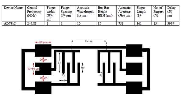
What Substrates/Wafers are used to Fabricate Multilayer Surface Acoustic Wave (SAW) Devices?
Researcher: We are working on the multilayer Surface acoustic wave (SAW) devices. Towards that we want to deposit thin film (1 to 5 microns) Aluminum nitride (AlN) on Si or SiC or any other substrate which can sustain temperature up to 500 Celsius, the substrate option is discussable. We aim to utilize piezoelectric properties of AlN, by depositing interdigital transduces (IDTs) on top of that. The options are discussable later. May you please let us know If you have such facility to address our requirements? We look forward to hearing from you soon.
UniversityWafer, Inc. Replied:
We can deposit thin film (1 to 5 microns) Aluminum nitride (AlN) on Silicon,SiC and Sapphire Substrate wafer,the wafer size available from 2'' to 8'',all these can sustain temperature up to 500 Celsius
Researcher:
Just let us know if you have photolithography facility there. After substrate preparation, we would need electrodes deposition. We will provide the mask for that.
UniversityWafer, Inc.
We have the photolithography facility. We can support to do the electrodes deposition.
Researcher:
We want to move on with SiC and Sphire substrates. Please share us the quotation including the photolithography services. For our case, 2" substrate will be better. As there will be multiple SAW devices on a single substrate, the dicing will be required at the end. Please give us a quotation, then we will be able to decide; how many substrates we can purchase in our budget.
It would be highly appreciated if we could get quotation on fast track.
The device above will be used as pressure sensor, and we need to make it stick to diaphragm which is inside a package.
We have this kind of scheme in our mind for the testing. Do your technical team give us suggestions on this? It would be great if could be done.

Researcher: I just want to summarize.
- The substrate need to be prepared on SiC with AlN thin film deposited on top of that.
- On top of substrate, SAW IDTs (IDT electrodes) will be fabricated.
The substrate is already finalized. For SAW fabrication, we need available list of photomasks (delay lines/resonator) as it was agreed before. From that list, we will choose one design and the payment process will be proceeded.
UniversityWafer, Inc. Quoted: Reference #265045 for pricing
Pls see below for the offer on each item,Just bare AlN template wafer,without additional process
1. thin film 2 microns Aluminum nitride (AlN) on 350um thick Double sides polished High Purity Semi insulating SiC substrate wafer,Qty. 10pcs
2. thin film 2 microns Aluminum nitride (AlN) on 430um thick Single side polished C-plane<0001> Sapphire substrate wafer,Qty. 10pcs
Regarding the additional cost of photolithography and deposit IDT electrodes,pls sharing us the process sequence or complete process procedures,So as to quote for your purpose,Our engineer asking for this.
What is Multilayer Surface Acoustic Wave Devices?
In this paper, we present a multilayer structure with piezoelectric aluminum nitride thin film, epitaxial cubic silicon carbide layer, and silicon substrate for strain sensing. We used alternating current reactive magnetron sputtering to deposit highly c-axis-oriented AlN thin films with full width at half maximum rocking curve of 1.36deg. We then fabricated conventional two-port SAW devices on this multilayer structure, and measured the SAW propagation properties.
The multilayer structure overcomes the material compatibility issue and increases the output power of the SAW device. This structure also has a high electromechanical coupling coefficient, higher resonant frequency, and reduced photolithography requirements. The advantages of multilayer structures over monolayer devices include their high output power, low complexity, and economic cost. We also show that multilayer devices have improved resonant frequency, low noise, and low power consumption.
This technology is also useful in mobile communication and in other applications. In mobile communication, SAW devices are used for resonators, filters, and microfluidics. A multilayer structure has multiple modes of SAWs, including high-order and bulk acoustic waves. Different design needs require different modes of surface waves. We will examine multilayer surface acoustic wave devices to determine their optimal applications.
The electromagnetic field of a surface acoustic wave is strongly influenced by its polarity. In this case, it is more effective to use a SAW that has a larger surface area. Multilayer surfaces can help detect the direction of sound and amplitude of acoustic waves. In addition to acoustic energy, surface acoustic devices can sense mass and mechanical properties.
What are IDT Electrodes?
If you are looking for an interdigital transducer for your ear, you will need to know what the electrodes are. Interdigital transducers have electrodes that can be changed to match different wavelengths. Changing the electrodes does not require any physical changes. They are also referred to as matched electrodes. You can match a pair of electrodes to each other to find the right one for your ear.
Different types of IDTs use different kinds of materials for their electrodes. The type of electrodes used determines the characteristics of the device. One type uses a comb-shaped top electrode. The other type generates waves by adding the phase electrodes and finger spacing. The wavelength of the generated beam depends on the length of the electrode fingers. This design is known as a T-IDT.
Nitrite ion detection can be done with nanogold film interdigital electrode sensors. These sensors detect nitrites quickly and conveniently. They can detect nitrites in food, body fluid, or blood. They are able to measure nitrites at a high enough level to be used for medical purposes. This type of electrode sensor also allows the measurement of nitrite in food and blood.
A comparison of A0 and S0 frequency responses reveals that the width of the electrodes has a greater influence on the A0 mode than the width of the interdigital electrodes. The two are related, as the ground electrodes are more prone to insertion loss. One study showed that the electrodes of FEUDTs were superconducting at 10 mK and thus eliminated resistive losses.
Full Charge Collection With Silicon Carbide Space Based Radiation Detector
In this article, we discuss the X-ray photon energy harvester response to high-energy irradiation and the advantages of silicon carbide (SiC) based radiation detectors. Other key features of SiC based radiation detectors include high sensitivity, Full charge collection, and high field withstandability. In addition, we will highlight the advantages of SiC based detectors in terms of performance and cost.
X-ray photon energy harvester response to high-energy irradiation
An x-ray photon energy harvester works by capturing and using the high-energy radiation. The  low-energy photons that are generated during X-ray radiation are not responsible for image formation. Instead, they are selectively filtered out by the body tissue. This results in lower levels of patient exposure and reduced radiation levels. In addition, X-ray photons are more prone to damage internal organs and tissues than low-energy photons.
To determine the sensitivity of a detector to X-ray radiation, the measurement team set up a test setup. The test system used a molybdenum tube that operated at 35 kV and five to thirty mA. The sample was positioned at 32 cm from the open shutter of the tube. The dose rate was measured to be from five to 29.9 mGy s-1.
X-rays are a form of electromagnetic radiation with a very short wavelength and high frequency. Their wavelength is approximately ten to twelve meters long, and the frequency is usually between 1016 and 20 hertz. The high-energy radiation that is emitted by high-energy particles is converted into electrons and ions that can be used for various applications. These particles are highly efficient for producing energy and are thus an ideal source of energy for renewable sources of energy.
An x-ray energy harvester can collect and store the energy from these photons. The wavelength of X-ray radiation is about ten to twelve meters and the energy of the photons can range from 100 eV to one MeV. These photons have the ability to penetrate through many different materials, including solids and liquids. Despite the high energy levels and short wavelengths, they are still used for medical applications.
The researchers demonstrated that the generated current signal was proportional to the volume of space charge region under a Schottky contact. This was a factor 106 higher than that reported in the literature. Further, they demonstrated that SiC Schottky diodes can be used as detectors for medical purposes without the need for external cooling. Moreover, they investigated the relationship between electrical characteristics of the diode and its spectroscopic response.
SiC based detectors have high sensitivity
The high sensitivity of SiC space based radiation detectors was achieved using a technique known as ion implantation. The particle can be irradiated using various particles, including 1 MeV neutrons. The electrical characterization of induced deep-level centers is a critical method for determining the main particle responsible for the degradation of the detector. The detectors are now being used in space radiation experiments.
In laboratory experiments, researchers have used the SiC detectors to measure the properties of multi-MeV ions in plasma. SiC detectors were fabricated by fabricating Schottky diodes on an 80 mm epitaxial layer. The detectors were fabricated with very low dopants, and were shown to cut visible and soft ultraviolet radiation. This increased their sensitivity to fast ions. Their time-of-flight spectra show the presence of peak signals corresponding to protons and different charge states.
The SiC space based radiation detectors exhibit good sensitivity and can be used in nuclear reactors and particle colliders. Because they do not depend on bias voltage, they are suitable for use in space radiation detection. However, the high sensitivity of these detectors is limited by their low leakage current and poor charge collection efficiency. Furthermore, the overall detector system requires a large cooling system, which increases its cost.
Another important characteristic of SiC space based radiation detectors is their low leakage currents. Leakage currents are very low. The measurements are carried out after the radiation tests. Moreover, the leakage currents of SiC space based radiation detectors are not affected by neutron radiation. So, SiC space based radiation detectors have good sensitivity and low leakage current.
The combination of high crystalline quality and high sensitivity makes SiC space based radiation detectors ideal for fusion devices and neutron detection. This material is also less susceptible to visible light, making it ideal for space applications. Moreover, it is cheaper, lighter, and more compact than its silicon-based counterparts. It also requires less power and is easier to handle. This combination of low cost, high sensitivity, and improved performance paves the way for more practical use.
Full charge collection
This full charge collection with silicon carbide space-based radiation detector has a wide range of potential applications in astrophysics. It is well-suited for neutron detection, as it can detect the particles at extremely low temperatures. This type of detector is also capable of high-temperature measurements. As a result, this detector has the potential to be an important tool in future missions. However, its development will depend on a variety of factors, including the ability to detect neutrons in low-temperature environments.
Despite the limitations of the fabricated detectors, these devices have a broad spectrum of applications, including particle and photon detectors. In the first experiment, different edge structures were tested, such as floating rings realized with JTE implanted rings and metal field plates. This first run of experiments was designed to test several edge structures, and subsequently, the fabrication process will be used for a thicker detector.
The main characteristic of SiC detectors is their ability to withstand a high internal electric field. These detectors are capable of handling eight to ten times the electric field of GaAs and Si, making them a promising option for high-voltage space missions. Further, the 4H-SiC material possesses a high breakdown field, which allows it to operate in the regime of saturated electron and hole drift velocity.
A number of benefits can be gained from this technology. In addition to the high sensitivity, it is able to combine high crystalline quality with full charge collection and low noise. Another benefit of SiC detectors is the absence of expensive cooling systems. The detectors also have lower cost, smaller size, lighter weight, and lower power consumption. The SiC space based radiation detectors are expected to perform better than silicon-based radiation detectors in the near future.
A silicon carbide detector consists of two layers, the dead layer and the active layer. The active layer is made of silicon and has a maximum thickness of 124 um. The detectors have the potential to detect alpha particles at a high energy. If these measurements are accurate, they could be used in astrophysics research program to study the effects of atomic particles on matter. If the technology becomes widely available, it would enable scientists to study the effects of atomic structures on our planet.
High field withstandability
Developed over many years, the Silicon Carbide space-based radiation detector is the ideal detector for neutron detection. Its high field withstandability makes it suitable for use in nuclear reactors and particle colliders. But the material's low intrinsic stability can pose a challenge to a space-based detector. It is expensive and requires an extensive cooling system. Its sensitivity is dependent on the depth of penetration of the reaction products.
The material is a superior choice for radiation detectors due to its ability to withstand high fields. The material's crystalline periodicity is disturbed by the presence of defects, introducing potential wells. The charge carriers can become trapped in these potential wells. Deep states are harder to escape than shallow states, and can be used for very high voltage devices. However, the device must have a high field withstandability.
The defect level of silicon carbide has a significant impact on the radiation sensitivity of this detector. Defects affect the capture cross section and carrier lifetime. They are also less prone to damage due to radiation. This makes them ideal for use in space-based radiation detectors. The sensitivity of the Silicon carbide space-based radiation detector depends on its energy withstandability. If this is the case, it can be used for radiation research.
The material's wide energy bandgap is another factor that contributes to its high radiation sensitivity. It also resists noise and leakage currents. Its high thermal conductivity allows it to dissipate excess heat, reducing operating temperature in close proximity to the detector. This increases the radiation hardness of the detector. High thermal conductivity also provides excellent thermal control.
The development team aims to produce unique compact radiation detectors for space missions. To do this, they have studied a variety of detector designs. They chose to use solid-state detectors because they have a lower operating voltage than traditional ones. This integration of technologies will improve the detector's performance. When it comes to detecting x-rays, this is a good option.
What is 3C Silicon Carbide?
If you are curious about this material, you may be wondering what is it, what its applications are, 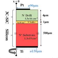 and why it is being used in aerospace. In this article, you will learn about its growth, properties, applications, and characteristics. You will also learn about its unique characteristics and properties, including its low thermal conductivity, which makes it a valuable material for advanced applications. Continue reading to find out more about 3C silicon carbide!
3C Silicon Carbide Growth
A new process for the epitaxial growth of 3C Silicon Carbide on Si substrates has been developed by researchers at the Queensland Micro and Nanotechnology Facility (QMF) of Griffith University and industry partner SPTS Technologies. The process has been demonstrated on 300mm silicon wafers and represents an impressive achievement. In addition to this research, the QMF has also developed a commercial reactor that can scale the process to commercial levels.
To create a 3C-SiC epitaxial layer, the substrate should have a cubic structure, a lattice parameter of 5% or less of 3C-SiC, and should be free of significant polytype and crystallographic transformations. The substrate should also exhibit excellent thermal conductivity and a high melting and dissociation temperature. Depending on the requirements of the application, the substrate may also have a high-quality substrate.
Because 3C-SiC has such great properties, it is an excellent candidate for semiconductor devices. Its high thermal conductivity and small bandgap make it well suited for semiconductor applications. Its ability to withstand high temperatures makes it an excellent material for high-density devices. And its superior properties enable it to be processed similarly to silicon devices. The polytype stability of 3C-SiC is a critical consideration for the fabrication of electronic devices.
A single-crystalline substrate capable of supporting 3C-SiC epitaxial layer is also necessary for growth. The substrate may be a metal carbide alloy having cubic crystal structure. Transition metal carbides are particularly well-suited to this method. The substrate must also be at a temperature of about 2700 degrees Celsius. The substrates used should be a minimum of 0.5 inches in diameter and must be compatible with the growth of 3C-SiC.
The process of growing 3C-SiC on a SiC surface is possible in a bubbler. Hydrogen flow through the bubbler can double the concentration of dopant in 3C-silicon carbide. Then, for each hydrogen flow through the bubbler, the growth rate is 0.6 micrometers per hour. During growth, undoped 3C-silicon carbide has a concentration of n-type carriers of 5 x 10¹⁶ per cubic centimeter. The nitrogen donors are thought to be responsible for this.
3C Silicon Caribide Properties
Three-C silicon carbide is a material with high potential for making high-temperature, high-power electrical devices. Its cubic polytype allows growth on cheap silicon substrates. This material's attractive chemical and physical properties make it a prime candidate for a wide variety of applications, including microelectromechanical systems. These unique properties have led to the development of many different types of devices, such as sensors and microelectronics.
Among all three C-SiC crystallinity phases, the zero-Burgers-vector triple dislocation complex (BED) exhibits the highest degree of stability, resulting in no strain introducing into the lattice. However, the local region of the complex core introduces strain. Thus, the SF has the most limited ability to modify 3C-SiC.
The fundamental mechanical and optical properties of SiC are essential in many industrial applications. These materials exhibit excellent thermal conductivity, chemical inertness, and defect characteristics. Their wide-ranging applications include high-power electronics, optical sensors, biomedical devices, and astronomical telescopes. Their nonlinear optical properties are also extensive, making them ideal materials for a wide range of applications. Moreover, they can be fabricated in challenging environments.
Molecular dynamics simulations of three-C silicon carbide crystals were used to study the dislocation complexes. Both analytical and Vashishta potentials are used for describing the interaction between Si and C atoms. They show qualitatively similar scenarios for extended defects. There are two types of stable dislocation complexes: one with two 30 deg and one with 90deg. These two are referred to as "B" and "D" structures, respectively.
Although the 3C-SiC polymorphs are not yet commercially available, they have reached important headways in MEMS and electrical applications. This material offers a cost-effective solution for these challenges. The ability to grow 3C-SiC on silicon substrates is a significant factor in making these devices. These materials are promising candidates for applications ranging from photovoltaics to solar cells.
What are 3C Silicon Carbide Applications
The applications of 3C Silicon Carbide are remarkably diverse. In addition to its use in many industries, 3C-SiC is cheaper than hexagonal polytypes. However, these advantages are offset by reduced quality. Here are some of its most important applications. Read on to learn more about this material and how it can benefit your business. Weighing in at a mere 2 grams per cubic meter, 3C-SiC is a strong and versatile material, making it ideal for applications in many industries.
Electrical applications of 3C-SiC are largely due to its wide bandgap. This characteristic enables it to be used as a controllable conductor for current flow in devices. In addition, the semiconductor material is capable of forming ohmic contacts with a metal. Ohmic contacts allow current to flow in the electrical device, exhibiting negligible resistance. In contrast, rectifying contacts are only useful for a single voltage regime, and thereby have no effect on the current flow.
Other applications of 3C-SiC include a variety of electrochemical systems. Its high melting point and operative temperature make it an excellent choice for microelectromechanical systems. These properties make 3C-SiC a highly versatile material for many applications, from energy storage to biomedical/chemical sensors. Its high melting point and operative temperature are both important for building microsystems.
Three-dimensional microstructures are also possible with 3C-SiC. While a solid 3C-SiC molecule has a band gap of four to six angstroms, it is still a polycrystalline material. During growth, 3C-SiC can be grown on silicon substrates. These features allow for applications in the medical field. This material is also an excellent choice for solar cells.
Three-dimensional (3D) silicon carbide crystals are available in polycrystalline and amorphous forms. The most widely available silicon carbide is 3C-SiC, but there are other polymorphic forms of this material. The polymorphs of 3C-SiC include cubic, hexagonal, and rhombohedral crystals. Silicon carbide polytypes are defined by the stacking order of the Si and C atoms in the unit cell.
Characteristics
The cubic polytype of Silicon Carbide (or 3C-SiC) presents remarkable electrical and mechanical properties as well as nanostructures. These properties combine to make it an excellent material for semiconductor and other electrical devices. In particular, these materials have low leakage currents and on-state resistances, which are essential parameters in high-frequency applications. Furthermore, their thermal conductivity is three times higher than the thermal conductivity of silicon.
Various polytypes of SiC are present, including cubic, hexagonal and rhombohedral. Among these polytypes, only threeC-SiC is commercially available. Their differences include their electrical, optical, thermal, and mechanical properties. To understand the differences and similarities, let's first define the crystalline structure of 3C-SiC. A cubic polytype has a single crystal of silicon, while a hexagonal crystal has a single crystal with a ring structure.
A significant difference between 3C-SiC and SiC is the absence of interfacial voids. The interfacial voids in silicon substrates affect the design of 3C-SiC epilayer-based devices. This effect is caused by the fact that 3C-SiC on silicon substrates must undergo a first carbonization stage, where the silicon substrate is consumed to form a silicon seed.
A 3C-SiC on-Si power diode is a versatile material that can be used for a variety of applications. It can be used as ultra-thin membranes for e-beam applications, piezoresistive devices, temperature sensors, and LEDs. In addition, SiC-on-SiC provides epitaxial deposition compatibility and is a good material for hexagonal nitride growth.
A 3C-SiC sample was investigated by scanning spreading resistance microscopy (SSRM). This method revealed alternating layers with successive nitrogen doping levels of 1017 to 5 x 1018 cm-3. These layers are separated by nonintentionally doped layers. In addition, atomic force microscopy did not detect any defects. Moreover, the SSRM cartography clearly demonstrated the presence of electrical activity.
The extended defects of 3C-SiC are an important concern when it comes to electrical performance. Because current preferentially flows through these extended defects, the electrical performance of the material is severely compromised. These defects also contribute to low breakdown voltages and leakage currents. To solve these problems, 3C-SiC devices need to be optimized for low-cost substrates. Its unique physical and chemical properties make it an attractive material for many applications.
Video: 3C Silicon Carbide Explained
What Types of Chips Made of Silicon Carbide?
Silicon carbide is a semiconductor that comes in many different types. There are three different polytypes: cubic unit cell, hexagonal unit cell, and four-dimensional (H-SiC). Each polytype is composed of alternating cubic and hexagonal symmetry. The cubic unit cell is the most common type.
Power semiconductors
Silicon carbide is a type of material used in power semiconductors. Its properties make it an excellent material for power electronics, including higher voltage, higher currents, and better thermal conductivity. Silicon carbide devices are also faster to switch than silicon and more robust. Silicon carbide belongs to the wide band gap semiconductor family, which offers several advantages. For example, silicon carbide devices have a larger breakdown field strength and higher thermal conductivity than silicon. However, they cannot match the breakdown field strength of silicon, so they are better suited for higher voltage applications.
Silicon carbide and silicon are the most common types of semiconductor materials. Both are characterized by the fact that they can switch between being insulators and conductors. The ability to switch between states makes these materials essential for making transistors, the building blocks of modern electronics. Silicon carbide also has a larger bandgap than silicon, so it can withstand more electrical fields than silicon.
Silicon carbide is also useful in high-temperature environments. Its wide band-gap makes it possible to use higher switching frequencies in high-voltage applications. The material is also tolerant of higher temperatures. These properties make silicon carbide an excellent material for solar power modules and data center power supplies. Furthermore, it can also be used in electric vehicle drive converters.
Silicon carbide semiconductors are extremely compact and powerful. The material is also more efficient at high voltages. The main market for these materials is in electric vehicles. These devices can be used in higher voltages and higher frequencies, making them a superior choice for EV charging and longer driving ranges.
Silicon carbide is one of the oldest materials used in power electronics. It has been used in transistors for decades, but recent developments have made other materials with higher bandgaps useful for power electronics. A recent breakthrough was reported by Masataka Higashiwaki at the National Institute of Information and Communications Technology (NICT) in Japan. Higashiwaki also announced the discovery of a promising transistor made of gallium oxide. These new materials have higher bandgaps than silicon carbide and gallium nitride. Research in this field has progressed rapidly.
Mirror material for astronomical telescopes
Silicon carbide is an excellent material for telescope mirrors because of its high stiffness and low density. It also has low thermal expansion and thermal stability. It is also lightweight, which makes it a good material for astronomical telescopes. This material is also a good choice for large mirrors. The biggest advantage of this material is its low thermal expansion.
The properties of mirrors are determined by a combination of their optical and physical-mechanical properties. Because large optics are often designed for weight savings, the mirrors must be able to resist thermal expansion and remain rigid. The material's thermal expansion properties also determine additional requirements for mirror structure. Large astro-telescope mirrors and other optical components should be made of materials that have low thermal expansion.
Silicon carbide is used for primary mirrors in astronomical telescopes. Silicon carbide mirrors are manufactured in 12 segments, which are brazed together and machined to the necessary thickness and surface accuracy. Once the mirrors are assembled, they must be tested and calibrated to ensure their optical quality.
Silicon carbide mirrors have outstanding mechanical and thermal properties. These qualities make them an excellent material for space telescopes. It is used in the primary mirror of the Herschel Space Observatory, which is 3.5 meters in diameter. Several different types of silicon carbide mirrors are available.
SiC mirrors are also lightweight. They offer the stiffness and thermal stability of beryllium telescopes, but are also more affordable than beryllium or glass telescopes. Besides, they are resistant to cryogenic temperatures and are suitable for space telescopes.
Fused silica has a long history as an optical substrate. This material has the lowest CTE and strain at 4.5 K, and is also good for light-weighting. It is also a good choice for high-resolution astronomical telescopes. But it requires additional processing and extra care in manufacturing.
As with all optical materials, mirror manufacturing is a complex process. There are many variables that must be considered before a final choice can be made. The most important parameters are specific stiffness and thermal performance. In this context, the primary mirror should be made of a durable material with a relatively low thermal expansion.
Mirror for traction inverters
Researchers have developed a new type of mirror for traction inverters made of silicon carbide. The silicon carbide mirror substrate is subjected to surface modification. The MRF polishing depth of the modified SiC mirror determines its surface roughness. This process is combined with a CCOS small grinding head to increase surface accuracy and roughness.
A traction inverter is a complex system that consists of several components. The traction inverter is composed of a power management IC, a microcontroller, a high-power power module, a temperature-sensing element, and a DC-link capacitor. The traction inverter's most critical component is a high-power switch that controls the flow of current to the motor. To minimize the risk of a failure, the high-power switch is monitored and protected.
The development of new semiconductor technology is advancing in the industry. The use of silicon carbide in space-based systems is a significant new development. This new material offers the potential for rapid and cost-effective manufacturing of large optical systems. However, it is still in its infancy and has little flight heritage. Thus, the development of a space-qualified silicon carbide mirror requires a rigorous qualification program. This qualification program requires a multidisciplinary approach and a large amount of financial investment.
The new mirror for traction inverters is a multifunctional device. Its multifunction capabilities allow it to be used in a wide range of electric vehicle applications. It also has an integrated pin fin baseplate, which allows direct liquid cooling. The high-quality silicon carbide inverter is also easy to assemble and offers superior thermal dissipation.
Another benefit of the silicon carbide mirror for traction inverters is that it offers protection and diagnostic capabilities. This makes it possible to monitor the system's performance and ensure that it is functioning properly. In addition, it is equipped with a dual-stage "active short circuit" protection system. This ensures that the system will not commutate without intention. It also prevents accidental motor shutdown.
The new mirror for traction inverters uses the latest SiC technology, which has improved the reliability and cost efficiency of traction inverters. Its thermal and mechanical properties have made silicon carbide a material of great interest for space instruments. The latest research is underway to refine the techniques used to manufacture silicon carbide mirrors.
MOSFETs
MOSFETs made of silicon carbide offer a number of benefits over their silicon counterparts. They offer higher breakdown voltage, better thermal conductivity, and smaller package sizes. They also have lower resistivity and recovery loss. As a result, silicon carbide MOSFETs have been widely used in power electronics applications.
These devices are ideal for use in hard-switching and resonant-switching topologies. They are also easy to drive and offer high-level efficiency at high switching frequencies. They are highly reliable and have a long lifetime.
Silicon carbide MOSFETs have higher drift doping than their silicon counterparts, enabling them to handle higher voltages. The difference in doping concentration leads to greater space charge capacitance, and this is an important property for high-power MOSFETs. High-voltage SiC MOSFETs are made with a smaller die size, and the amount of doping in the N-layer increases the transfer capacitance.
Silicon carbide is more abundant than silicon and has lower up-front cost. Its low neutron cross-section makes it useful in nuclear reactor applications, and its low permeability makes it highly resistant to radiation. It is also used in mould coating for batch casting molten metals.
Silicon carbide power devices enable significant improvements to existing power applications, and enable new ones. This is because of SiC's outstanding material properties, such as high thermal conductivity, low intrinsic carrier concentration, and chemical inertness. It is also advantageous for high-temperature electronics and for applications in harsh environments. Because of its low output capacitance, SiC-based devices are ideal for switching applications.
Video: Silicon Caribide MOSFETS
How are Silicon Carbide (SiC) Wafers Made?
Silicon carbide (SiC) wafers are made using a process called sublimation. The process involves using a silicon carbide crystal as a seed crystal, which is placed in a chamber with a mixture of silicon and carbon. The chamber is then heated to a high temperature, causing the silicon and carbon to vaporize and form a gas. As the gas cools, it condenses onto the seed crystal, forming a layer of silicon carbide.
This process is repeated multiple times, with each layer being carefully controlled in terms of thickness and composition, until the desired thickness and quality of the wafer is achieved. The wafer is then polished and cut into the desired shape and size.
SiC wafers are used in a variety of applications, including the production of power electronic devices, high-temperature sensors, and high-strength ceramics. They are known for their high thermal conductivity, high breakdown strength, and high-temperature stability, which make them ideal for use in harsh environments and high-power applications.