
Are Test Grade Silicon Wafers Suitable for Research?
Test grade silicon wafers are often a cost-effective choice for process development, thin-film deposition, equipment qualification, and other experiments that do not require the tighter surface-quality limits of prime grade material. The correct grade depends on what will be measured, the sensitivity of the process, and the cleanliness requirements of the tool.
A researcher asked whether test grade wafers could be used to measure deposition rate, film uniformity, and refractive index during sputtering, PECVD, and LPCVD processes. The researcher also needed dummy wafers to fill unused positions in an LPCVD wafer boat.
Short answer: test grade wafers are commonly suitable for deposition-monitoring work, provided their surface condition and specifications are compatible with the measurement method. Mechanical grade wafers may be acceptable as non-measurement dummies, but only after confirming that their dopant, cleanliness, geometry, and prior processing are permitted in the deposition tool.
Get Your Test Grade Silicon Wafer Quote FAST! Or, Buy Online and start researching today.
Test Grade vs. Prime Grade Silicon Wafers
A wafer grade is not determined by one property alone. Diameter, thickness, total thickness variation, bow, warp, crystal orientation, conductivity type, dopant, resistivity, surface finish, particles, scratches, and other defects can all affect whether a wafer is appropriate for a specific process.
Prime grade silicon wafers are generally preferred for device fabrication, photolithography, epitaxy, advanced optical measurements, and other defect-sensitive processes. Their tighter surface and dimensional specifications help reduce variability when small particles, scratches, haze, or crystal defects could affect yield or data.
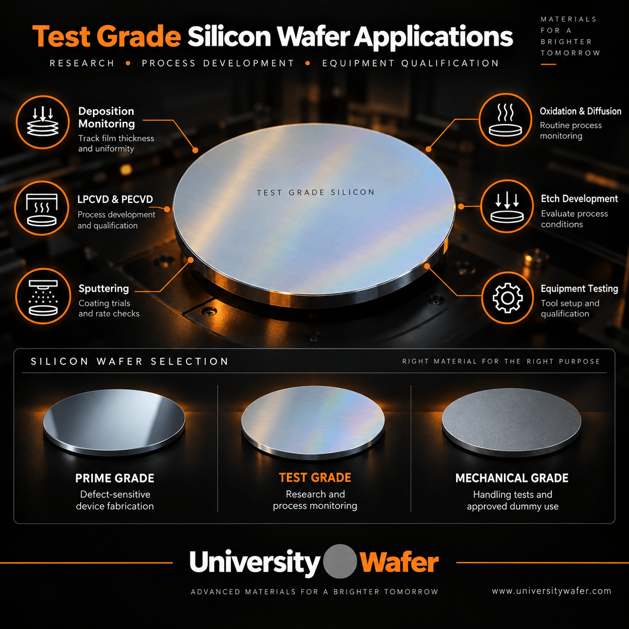
Test grade wafers may have less restrictive cosmetic specifications while still providing controlled electrical, crystallographic, dimensional, and surface properties. They are frequently used as monitor wafers for film deposition, oxidation, diffusion, coating trials, etch development, and equipment testing.
For deposition-rate or uniformity measurements, choose wafers with a surface finish compatible with the metrology technique. Refractive index is a property of the deposited film, but techniques such as ellipsometry also depend on an appropriate optical model and a sufficiently smooth, clean substrate. A test wafer with scratches, heavy haze, particles, or unknown surface films may not be suitable for precise optical measurements.
Can Mechanical Grade Wafers Be Used as LPCVD Dummies?
Mechanical grade wafers may be used as spacers or dummy wafers when no measurements or devices will be made on them. However, mechanical grade does not automatically mean that a wafer is clean enough for a semiconductor furnace. Confirm the material history, dopant, surface condition, dimensions, and cleanliness before introducing it into an LPCVD or PECVD system.
Tool-specific contamination rules are especially important in shared or high-temperature equipment. Certain dopants, metals, particles, residues, or previously deposited films may be prohibited because they can contaminate the chamber or other wafers. Always follow the process owner’s approved-material list and cleaning procedure.
Repeatedly coated dummy wafers can eventually shed particles when accumulated films develop excessive stress or poor adhesion. This risk depends mainly on the deposited material, total film thickness, thermal cycling, wafer surface, and handling—not simply on whether the starting wafer was labeled test or mechanical grade. Replace coated dummies according to the tool’s maintenance procedure before cracking or flaking occurs.
How to Select the Right Wafer Grade
- Use prime grade for device fabrication, fine lithography, epitaxy, or measurements that require tight control of surface defects and geometry.
- Use test grade for deposition monitoring, process development, oxidation, diffusion, etching, coating trials, and many routine research applications.
- Consider mechanical grade for handling tests, equipment setup, spacers, or non-measurement dummies when the tool’s contamination and dimensional requirements allow it.
Before ordering, specify the required diameter, thickness, orientation, conductivity type, dopant, resistivity, polish, quantity, and intended process. If the wafer will enter a high-temperature or contamination-sensitive tool, include the tool’s approved-material requirements with the quote request.
Click the image below to visit our store. Buy as few as one wafer.
Test Grade Silicon Wafers in Thin-Film Research
Silicon wafers are widely used as rigid, smooth substrates for polymer and thin-film experiments. In one surface-mechanics application, polystyrene films were spin-coated onto ultraviolet/ozone-treated silicon wafers. Changing the polymer concentration and spin speed produced films with different thicknesses, which were then characterized using optical measurements.
This type of work illustrates why researchers often select test grade silicon: it can provide a consistent, polished substrate for coating and characterization without requiring device-grade material. The wafer must still be sufficiently clean and smooth for the intended film thickness and measurement technique.
Example Wafer Specification
Si Item #452
100mm diameter, P-type, (100) orientation, 0–100 Ohm-cm resistivity,
single-side polished, 500 µm thickness, test grade.
Product availability and exact specifications may change. Confirm the current specification and suitability for your process before ordering.
Test Grade Silicon Wafer Specifications
UniversityWafer offers test grade silicon wafers for semiconductor research, process development, equipment qualification, and thin-film deposition monitoring. Available configurations may include P-type, N-type, and undoped silicon with different dopants, crystal orientations, resistivity ranges, thicknesses, and polished surface options.
Test grade wafers are a practical choice when a consistent silicon substrate is needed but the tighter cosmetic requirements of prime grade material are not necessary. Common applications include LPCVD, PECVD, sputtering, oxidation, diffusion, coating trials, and routine equipment tests.
Buy test grade silicon wafers online or contact us for help selecting a substrate for your process.
100mm Test Grade Silicon Wafers
The table below lists 100mm test grade wafer configurations. Compare conductivity type, dopant, crystal orientation, polish, primary-flat geometry, resistivity, and wafer thickness.
Diameter (mm) |
Type |
Dopant |
Orientation |
Polish |
Primary Flat Length |
Primary Flat Direction |
Resistivity (Ohm-cm) |
Thickness (µm) |
| 100.0 ± 0.5 | N+ | Sb | 100 | DSP | 32.5 ± 2.5 | 110 ± 1 | 0.010 - 0.020 | 340 ± 10 |
| 100 ± 0.5 | N+ | Sb | 100 | DSP | 32.5 ± 2.5 | 110 ± 0,20 | 0.010 - 0.025 | 300 ± 5 |
| 100.0 ± 0.5 | N+ | Sb | 100 | DSP | 32.5 ± 2.5 | 110 ± 0,50 | 0.010 - 0.022 | 310 ± 5 |
| 100 ± 0.2 | N+ | Sb | 100 | DSP | 32.5 ± 2.5 | 110 ± 1 | 0.005 - 0.020 | 300 ± 2.5 |
| 100.0 ± 0.5 | N+ | Sb | 100 | DSP | 32.5 ± 2.5 | 110 ± 0,50 | 0.008 - 0.022 | 400 ± 10 |
| 100.0 ± 0.5 | N+ | Sb | 100 | DSP | 32.5 ± 2.5 | 110 ± 0,50 | 0.01 - 0.03 | 600 ± 15 |
| 100.0 ± 0.5 | N+ | Sb | 100 | DSP | 32.5 ± 2.5 | 110 ± 0,50 | 0.01 - 0.02 | 420 ± 5 |
| 100.0 ± 0.5 | N+ | Sb | 100 | DSP | 32.5 ± 2.5 | 110 ± 0,50 | 0.01 - 0.02 | 520 ± 5 |
| 100 ± 0.5 | N+ | Sb | 100 | DSP | 32.5 ± 2.5 | 110 ± 0,20 | 0.010 - 0.025 | 315 ± 5 |
| 100.0 ± 0.5 | N+ | Sb | 100 | DSP | 32.5 ± 2.5 | 110 ± 0,50 | 0.01 - 0.02 | 420 ± 5 |
| 100.0 ± 0.5 | N+ | Sb | 100 | DSP | 32.5 ± 2.5 | 110 ± 1 | 0.010 - 0.020 | 380 ± 10 |
| 100.0 ± 0.5 | N+ | Sb | 100 | DSP | 32.5 ± 2.5 | 110 ± 1 | 0.010 - 0.020 | 355 ± 10 |
| 100.0 ± 0.5 | N+ | Sb | 100 | DSP | 32.5 ± 2.5 | 110 ± 1 | 0.010 - 0.020 | 500 ± 10 |
| 100 ± 0.5 | N+ | Sb | 100 | DSP | 32.5 ± 2.5 | 110 ± 0,20 | 0.010 - 0.025 | 300 ± 5 |
| 100 ± 0.5 | N+ | Sb | 100 | DSP | 32.5 ± 2.5 | 110 ± 1 | 0.005 - 0.020 | 525 ± 25 |
| 100 ± 0.5 | N+ | Sb | 100 | DSP | 32.5 ± 2.5 | 110 ± 1 | 0.005 - 0.020 | 525 ± 25 |
| 100 ± 0.5 | N+ | Sb | 100 | DSP | 32.5 ± 2.5 | 110 ± 0,50 | 0.010 - 0.025 | 315 ± 3 |
| 100.0 ± 0.5 | N+ | Sb | 100 | DSP | 32.5 ± 2.5 | 110 ± 1 | 0.010 - 0.020 | 380 ± 10 |
| 100 ± 0.2 | N+ | Sb | 100 | DSP | 32.5 ± 2.5 | 110 ± 1 | 0.005 - 0.020 | 300 ± 2.5 |
| 100.0 ± 0.5 | N+ | Sb | 100 | DSP | 32.5 ± 2.5 | 110 ± 1 | 0.010 - 0.020 | 380 ± 10 |
| 100 ± 0.5 | N+ | As | 100 | DSP | 32.5 ± 2.5 | 110 ± 0,50 | 0.001 - 0.005 | 380 ± 10 |
| 100.0 ± 0.3 | P+ | B | 100 | DSP | 32.5 ± 2.5 | 110 ± 0,50 | 0.01 - 0.020 | 327 ± 5 |
| 100.0 ± 0.3 | P+ | B | 100 | DSP | 32.5 ± 2.5 | 110 ± 1 | 0.015 - 0.020 | 381 ± 7 |
| 100 ± 0.5 | P+ | B | 100 | DSP | 32.5 ± 2.5 | 110 ± 0,50 | 0.01 - 0.02 | 525 ± 25 |
| 100 ± 0.5 | P | B | 100 | DSP | 32.5 ± 2.5 | 110 ± 1 | 0.5 - 10 | 318 ± 12.7 |
| 100 ± 0.15 | P | B | 110 | DSP | 32.5 ± 2.5 | 111 ± 0,10 | 5--10 | 200 ± 15 |
| 100 ± 0.5 | P+ | B | 100 | DSP | 32.5 ± 2.5 | 110 ± 1 | 0.010 - 0.020 | 200 ± 10 |
| 100 ± 0.38 | P | B | 100 | DSP | 32.5 ± 2.5 | 110 ± 0,50 | 0.5 - 10 | 889 ± 12.7 |
| 100.0 ± 0.2 | P | B | 100 | DSP | 32.5 ± 2.5 | 110 ± 1 | 0.1 - 0.5 | 380 ± 5 |
| 100 ± 0.38 | P | B | 100 | DSP | 32.5 ± 2.5 | 110 ± 1 | 0.5 - 10 | 508 ± 12.7 |
| 100 ± 0.5 | P | B | 111 | DSP | 32.5 ± 2.5 | 110 ± 1 | 10--20 | 525 ± 25 |
| 100.0 ± 0.2 | P | B | 100 | DSP | 32.5 ± 2.5 | 110 ± 0,50 | 8--10 | 225 ± 10 |
| 100 ± 0.5 | P | B | 100 | DSP | 32.5 ± 2.5 | 110 ± 1 | 3--5 | 350 ± 10 |
| 100 ± 0.3 | P | B | 100 | DSP | 32.5 ± 2.5 | 110 ± 0,50 | 1--5 | 225 ± 5 |
| 100 ± 0.5 | P | B | 100 | DSP | 32.5 ± 2.5 | 110 ± 1 | 1--20 | 350 ± 15 |
| 100 ± 0.2 | P+ | B | 100 | DSP | 32.5 ± 2.5 | 110 ± 0,30 | < 0.020 | 300 ± 15 |
| 100 ± 0.38 | P | B | 100 | DSP | 32.5 ± 2.5 | 110 ± 1 | 0.5 - 10 | 318 ± 12.7 |
| 100 ± 0.5 | P+ | B | 111 | DSP | 32.5 ± 2.5 | 110 ± 1 | 0.0034 - 0.004 | 450 ± 5 |
| 100 ± 0.15 | P | B | 110 | DSP | 32.5 ± 2.5 | 111 ± 0,10 | > 1 | 381 ± 15 |
| 100 ± 0.5 | P | B | 100 | DSP | 32.5 ± 2.5 | 110 ± 0,50 | 1--10 | 280 ± 10 |
| 100 ± 0.2 | P | B | 100 | DSP | 32.5 ± 2.5 | 110 ± 0,20 | 1--10 | 490 ± 5 |
| 100 ± 0.5 | P | B | 100 | DSP | 32.5 ± 2.5 | 110 ± 0,50 | 5--10 | 525 ± 5 |
| 100 ± 0.5 | P | B | 110 | DSP | 32.5 ± 2.5 | 111 ± 0,20 | 5--10 | 380 ± 5 |
| 100.0 ± 0.5 | P | B | 100 | DSP | 32.5 ± 2.5 | 110 ± 1 | 5--7 | 483 ± 25 |
| 100 ± 0.2 | P | B | 100 | DSP | 32.5 ± 2.5 | 110 ± 0,20 | 2--4 | 280 ± 5 |
| 100 ± 0.5 | P | B | 100 | DSP | 32.5 ± 2.5 | 110 ± 0,50 | 3--7 | 300 ± 5 |
| 100 ± 0.3 | P | B | 100 | DSP | 32.5 ± 2.5 | 110 ± 0,50 | 1--5 | 390 ± 10 |
| 100 ± 0.5 | P | B | 100 | DSP | 32.5 ± 2.5 | 110 ± 0,50 | 3--7 | 385 ± 5 |
| 100 ± 0.2 | P | B | 100 | DSP | 32.5 ± 2.5 | 110 ± 0,20 | 1--10 | 490 ± 20 |
| 100.0 ± 0.3 | P+ | B | 100 | DSP | 32.5 ± 2.5 | 110 ± 1 | 0.015 - 0.020 | 381 ± 7 |
| 100 ± 0.3 | P | B | 100 | DSP | 32.5 ± 2.5 | 110 ± 1 | 1 - 100 | 202 ± 4 |
| 100 ± 0.3 | P | B | 100 | DSP | 32.5 ± 2.5 | 110 ± 1 | 1 - 100 | 302 ± 4 |
| 100 ± 0.5 | P | B | 100 | DSP | 32.5 ± 2.5 | 110 ± 0,50 | 3--7 | 385 ± 5 |
| 100 ± 0.2 | P+ | B | 100 | DSP | 32.5 ± 2.5 | 110 ± 0,50 | 0.010 - 0.025 | 500 ± 25 |
| 100 ± 0.5 | N | Ph | 100 | DSP | 32.5 ± 2.5 | 110 ± 1 | 0.5 - 1.0 | 385 ± 5 |
| 100.0 ± 0.5 | N | Ph | 111 | DSP | 32.5 ± 2.5 | 110 ± 0,20 | 1--10 | 300 ± 3 |
| 100 ± 0.5 | N | Ph | 100 | DSP | 32.5 ± 2.5 | 110 ± 0,20 | 2--4 | 260 ± 2 |
| 100 ± 0.5 | N | Ph | 100 | DSP | 32.5 ± 2.5 | 110 ± 0,20 | 2--4 | 300 ± 2 |
| 100.0 ± 0.5 | N | Ph | 100 | DSP | 32.5 ± 2.5 | 110 ± 1 | 1--10 | 350 ± 15 |
| 100.0 ± 0.5 | N | Ph | 100 | DSP | 32.5 ± 2.5 | 110 ± 1 | 3--5 | 525 ± 5 |
| 100 ± 0.5 | N | Ph | 111 | DSP | 32.5 ± 2.5 | 110 ± 0,50 | 3--8 | 450 ± 10 |
| 100 ± 0.5 | N | Ph | 100 | DSP | 32.5 ± 2.5 | 110 ± 0,20 | 2--4 | 220 ± 2 |
| 100 ± 0.5 | N | Ph | 100 | DSP | 32.5 ± 2.5 | 110 ± 1 | 1--3 | 368 ± 10 |
| 100 ± 0.2mm | N | Ph | 100 | DSP | 32.5 ± 2.5 | 110 ± 0,20 | 0.20 - 0.25 | 380 ± 5 |
| 100.0 ± 0.5 | N | Ph | 100 | DSP | 32.5 ± 2.5 | 110 ± 1 | 2--6 | 381 ± 6 |
| 100.0 ± 0.5 | N | Ph | 111 | DSP | 32.5 ± 2.5 | 110 ± 0,50 | 1--10 | 350 ± 3 |
| 100.0 ± 0.5 | N | Ph | 100 | DSP | 32.5 ± 2.5 | 110 ± 1 | 10--20 | 300 ± 10 |
| 100 ± 0.5 | N | Ph | 100 | DSP | 32.5 ± 2.5 | 110 ± 0,50 | 1.4 - 6.0 | 445 ± 5 |
| 100.0 ± 0.5 | N | Ph | 100 | DSP | 32.5 ± 2.5 | 110 ± 1 | 5--8 | 300 ± 5 |
| 100 ± 0.5 | N | Ph | 100 | DSP | 32.5 ± 2.5 | 110 ± 1 | 1--3 | 368 ± 10 |
| 100 ± 0.5 | N | Ph | 100 | DSP | 32.5 ± 2.5 | 110 ± 1 | 0.05 - 0.5 | 525 ± 25 |
| 100.0 ± 0.5 | N | Ph | 100 | DSP | 32.5 ± 2.5 | 110 ± 0,50 | 3--5 | 300 ± 5 |
| 100 ± 0.5 | N | Ph | 100 | DSP | 32.5 ± 2.5 | 110 ± 0,20 | 2--4 | 400 ± 2 |
| 100.0 ± 0.5 | N | Ph | 100 | DSP | 32.5 ± 2.5 | 110 ± 1 | 10--20 | 300 ± 10 |
| 100 ± 0.5 | N | Ph | 100 | DSP | 32.5 ± 2.5 | 110 ± 0,50 | 3--5 | 200 ± 4 |
| 100.0 ± 0.5 | N | Ph | 100 | DSP | 32.5 ± 2.5 | 110 ± 0,50 | 1--10 | 500 ± 15 |
| 100 ± 0.5 | N | Ph | 100 | DSP | 32.5 ± 2.5 | 110 ± 0,25 | 1--10 | 300 ± 5 |
| 100 ± 0.5 | N | Ph | 100 | DSP | 32.5 ± 2.5 | 110 ± 0,20 | 1 - 100 | 360 ± 10 |
| 100.0 ± 0.5 | N | Ph | 100 | DSP | 32.5 ± 2.5 | 110 ± 0,50 | 1--10 | 380 ± 5 |
| 100 ± 0.2 | N | Ph | 100 | DSP | 32.5 ± 2.5 | 110 ± 0,50 | 1--10 | 350 ± 5 |
| 100 ± 0.5 | N | Ph | 100 | DSP | 32.5 ± 2.5 | 110 ± 1 | 1--3 | 280 ± 5 |
| 100 ± 0.5 | N | Ph | 100 | DSP | 32.5 ± 2.5 | 110 ± 1 | 0.05 - 0.5 | 525 ± 25 |
| 100 ± 0.2 | N | Ph | 100 | DSP | 32.5 ± 2.5 | 110 ± 0,30 | 2--10 | 380 ± 5 |
| 100.0 ± 0.2 | N | Ph | 100 | DSP | 32.5 ± 2.5 | 110 ± 1 | 0.04 - 20 | 400 ± 10 |
| 100 ± 0.2 | N | Ph | 100 | DSP | 32.5 ± 2.5 | 110 ± 0,30 | 2--10 | 300 ± 5 |
| 100.0 ± 0.5 | N | Ph | 100 | DSP | 32.5 ± 2.5 | 110 ± 0,50 | 3--5 | 525 ± 5 |
| 100 ± 0.5 | N | Ph | 100 | DSP | 32.5 ± 2.5 | 110 ± 0,50 | 0.5 - 1.0 | 485 ± 5 |
| 100 ± 0.5 | N | Ph | 100 | DSP | 32.5 ± 2.5 | 110 ± 0,50 | 0.5 - 1.0 | 385 ± 5 |
| 100.0 ± 0.5 | N | Ph | 100 | DSP | 32.5 ± 2.5 | 110 ± 1 | 10--20 | 300 ± 10 |
| 100 ± 0.25 | N+ | Red Ph | 100 | DSP | 32.5 ± 2.5 | 110 ± 0,20 | < 0.0015 | 250 ± 5 |
| 100 ± 0.25 | N+ | Red Ph | 100 | DSP | 32.5 ± 2.5 | 110 ± 0,50 | < 0.0015 | 380 ± 5 |
| 100 ± 0.3 | N+ | As | 111 | SSP | 32.5 ± 2.5 | 110 ± 1 | < 0.005 | 381 ± 15 |
150mm Test Grade Silicon Wafers
These 150mm options support process development, deposition monitoring, equipment testing, and other laboratory or production-support applications. Select the electrical and mechanical properties that match your process.
Diameter (mm) |
Type |
Dopant |
Orientation |
Polish |
Primary Flat Length |
Primary Flat Direction |
Resistivity (Ohm-cm) |
Thickness (µm) |
| 150.0 ± 0.2 | N+ | Sb | 100 | DSP | 57.5 ± 2.5 | 110 ± 0,30 | 0.005 - 0.020 | 380 ± 5 |
| 150 ± 0.2 | N+ | Sb | 100 | DSP | 57.5 ± 2.5 | 110 ± 1 | 0.005-0.02 | 215-235 |
| 150.0 ± 0.2 | N+ | Sb | 100 | DSP | 57.5 ± 2.5 | 011 ± 0,30 | 0.005 - 0.020 | 380 ± 5 |
| 150 ± 0.2 | N+ | Sb | 100 | DSP | 57.5 ± 2.5 | 110 ± 0,10 | < 0.020 | 400 ± 10 |
| 150 ± 0.2 | N+ | Sb | 100 | DSP | 57.5 ± 2.5 | 110 ± 0,50 | 0.01 - 0.02 | 400 ± 15 |
| 150 ± 0.5 | N+ | Sb | 100 | DSP | 57.5 ± 2.5 | 110 ± 0,50 | 0.01 - 0.02 | 425 ± 5 |
| 150.0 ± 0.2 | N+ | Sb | 100 | DSP | 57.5 ± 2.5 | 110 ± 0,30 | 0.005 - 0.020 | 380 ± 5 |
| 150.0 ± 0.2 | N+ | Sb | 100 | DSP | 57.5 ± 2.5 | 011 ± 0,30 | 0.005 - 0.020 | 380 ± 5 |
| 150.0±0.2 | N+ | Sb | 100 | DSP | 57.5 ± 2.5 | 110 ± 0,20 | 0.010-0.020 | 375-385 |
| 150 ± 0.2 | N+ | Sb | 100 | DSP | 57.5 ± 2.5 | 110 ± 0,50 | 0.01 - 0.02 | 325 ± 5 |
| 150 ± 0.2 | N+ | Sb | 100 | DSP | 57.5 ± 2.5 | 110 ± 0,50 | 0.01 - 0.02 | 300 ± 10 |
| 150.0 ± 0.2 | N+ | As | 100 | DSP | 57.5 ± 2.5 | 110 ± 1 | <0.0035 | 430 ± 5 |
| 150.0 ± 0.2 | N+ | As | 100 | DSP | 57.5 ± 2.5 | 110 ± 1 | <0.0035 | 430 ± 5 |
| 150 ± 0.2mm | P+ | B | 100 | DSP | 57.5 ± 2.5 | 110 ± 1 | 0.005 - 0.025 | 400 ± 10 |
| 150 ± 0.2 | P | B | 100 | DSP | 57.5 ± 2.5 | 110 ± 0,50 | 1 - 20 | 400 ± 5 |
| 150 ± 0.2 | P | B | 100 | DSP | 57.5 ± 2.5 | 110 ± 0,50 | 2.55 - 3.45 | 400 ± 10 |
| 150 ± 0.2 | P | B | 100 | DSP | 57.5 ± 2.5 | 110 ± 0,20 | 1--5 | 650 ± 5 |
| 150 ± 0.2 | P+ | B | 100 | DSP | 57.5 ± 2.5 | 110 ± 0,20 | 0.017 - 0.022 | 381 ± 5 |
| 150 ± 0.2 | P | B | 100 | DSP | 57.5 ± 2.5 | 110 ± 1 | >1 | 525 ± 12.5 |
| 150 ± 0.2 | P | B | 100 | DSP | 57.5 ± 2.5 | 110 ± 0,50 | 1--5 | 450 ± 10 |
| 150.0 ± 0.2 | P+ | B | 100 | DSP | 57.5 ± 2.5 | 110 ± 0,50 | 0.007 - 0.020 | 400 ± 25 |
| 150 ± 0.2 | P+ | B | 100 | DSP | 57.5 ± 2.5 | 110 ± 0,50 | < 0,005 | 625 ± 15 |
| 150 ± 0.5 | P | B | 100 | DSP | 57.5 ± 2.5 | 110 ± 0,50 | 1--10 | 500 ± 25 |
| 150 ± 0.2 | P | B | 100 | DSP | 57.5 ± 0.5 | 110 ± 0,30 | 2--10 | 380 ± 4 |
| 150 ± 0.2 | P | B | 100 | DSP | 57.5 ± 2.5 | 110 ± 0,50 | 1--10 | 600 ± 5 |
| 150 ± 0.2 | P | B | 100 | DSP | 57.5 ± 2.5 | 110 ± 0,10 | 0.07 - 0.13 | 500 ± 5 |
| 150 ± 0.2 | P | B | 100 | DSP | 57.5 ± 2.5 | 110 ± 0,20 | 1--5 | 300 ± 5 |
| 150 ± 0.2 | P+ | B | 100 | DSP | 57.5 ± 2.5 | 110 ± 1 | 0.001 - 0.02 | 650 ± 5 |
| 150.0 ± 0.2 | P | B | 100 | DSP | 57.5 ± 2.5 | 110 ± 1 | 6 - 8.5 | 380 ± 5 |
| 150 ± 0.2 | P+ | B | 100 | DSP | 57.5 ± 2.5 | 110 ± 1 | 0.020 - 0.025 | 300 ± 7.5 |
| 150 ± 0.2 | P | B | 100 | DSP | 57.5 ± 2.5 | 110 ± 0,10 | 2.4 - 3.6 | 400 ± 10 |
| 150 ± 0.5 | P | B | 100 | DSP | 57.5 ± 0.5 | 110 ± 0,30 | > 0.3 | 400 ± 50 |
| 150.0 ± 0.2 | P | B | 100 | DSP | 57.5 ± 2.5 | 110 ± 0,50 | 6 - 8.5 | 380 ± 10 |
| 150 ± 0.5 | P | B | 100 | DSP | 57.5 ± 2.5 | 110 ± 0,20 | 1--5 | 400 ± 5 |
| 150.0 ± 0.2 | P | B | 100 | DSP | 57.5 ± 2.5 | 110 ± 0,10 | 0.07 - 0.13 | 380 ± 5 |
| 150 ± 0.2 | P+ | B | 100 | DSP | 57.5 ± 2.5 | 110 ± 0,50 | 0.010 - 0.020 | 1000 ± 5 |
| 150 ± 0.3 | P | B | 100 | DSP | 57.5 ± 2.5 | 110 ± 0,50 | 30 - 50 | 300 ± 5 |
| 150 ± 0.2 | P | B | 100 | DSP | 57.5 ± 2.5 | 110 ± 1 | 2 - 20 | 310 ± 10 |
| 150 ± 0.2 | P+ | B | 100 | DSP | 57.5 ± 2.5 | 110 ± 1 | 0.005 - 0.025 | 290 ± 10 |
| 150 ± 0.2 | P+ | B | 100 | DSP | 57.5 ± 2.5 | 110 ± 1 | 0.005 - 0.025 | 400 ± 10 |
| 150 ± 0.5 | P | B | 100 | DSP | 57.5 ± 2.5 | 110 ± 1 | 5 - 8.5 | 525 ± 5 |
| 150 ± 0.5 | P | B | 100 | DSP | 57.5 ± 2.5 | 110 ± 1 | 3--5 | 390 ± 7 |
| 150 ± 0.5 | P | B | 100 | DSP | 57.5 ± 2.0 | 110 ± 1 | 5 - 8.5 | 525 ± 5 |
| 150 ± 0.2 | P | B | 100 | DSP | 47.5 ± 2.5 | 110 ± 0,50 | 3--7 | 385 ± 5 |
| 150 ± 0.2 | P | B | 100 | DSP | 57.5 ± 2.5 | 110 ± 0,20 | 1--10 | 400 ± 5 |
| 150 ± 0.2 | P | B | 100 | DSP | 57.5 ± 2.5 | 110 ± 0,20 | 1--10 | 600 ± 5 |
| 150 ± 0.5 | P | B | 100 | DSP | 47.5 ± 2.5 | 110 ± 0,50 | 70 - 130 | 1000 ± 10 |
| 150 ± 0.2 | P | B | 100 | DSP | 57.5 ± 2.5 | 110 ± 0,50 | 1 - 10 | 400 ± 5 |
| 150 ± 0.5 | P | B | 100 | DSP | 57.5 ± 2.5 | 110 ± 0,25 | 1--10 | 280 ± 1.5 |
| 150 ± 0.2 | P | B | 100 | DSP | 57.5 ± 2.5 | 110 ± 0,20 | 1--10 | 650 ± 5 |
| 150 ± 0.5 | P | B | 100 | DSP | 57.5 ± 2.5 | 110 ± 1 | 5 - 8.5 | 400 ± 5 |
| 150 ± 0.5 | P | B | 100 | DSP | 57.5 ± 2.5 | 100 ± 0,50 | 5--7 | 483 ± 5 |
| 150.0 ± 0.5 | P | B | 100 | DSP | 57.5 ± 2.5 | 110 ± 1 | 5 - 8.5 | 380 ± 5 |
| 150 ± 0.5 | P | B | 100 | DSP | 57.5 ± 2.5 | 110 ± 0,50 | 1--10 | 600 ± 5 |
| 150 ± 0.5 | P+ | B | 100 | DSP | 57.5 ± 2.5 | 110 ± 0,50 | 0.01 - 0.02 | 620 ± 5 |
| 150 ± 0.2 | P | B | 100 | DSP | 57.5 ± 2.5 | 110 ± 0,10 | 1--10 | 600 ± 5 |
| 150 ± 0.5 | P | B | 100 | DSP | 57.5 ± 2.5 | 110 ± 0,50 | > 10 | 625 ± 15 |
| 150 ± 0.5 | P | B | 100 | DSP | 57.5 ± 2.5 | 110 ± 1 | 1--3 | 380 ± 12 |
| 150 ± 0.5 | P | B | 100 | DSP | 57.5 ± 2.5 | 110 ± 1 | 5 - 8.5 | 525 ± 5 |
| 150 ± 0.2 | P | B | 100 | DSP | 57.5 ± 2.5 | 110 ± 0,10 | 2.4 - 3.6 | 400 ± 10 |
| 150 ± 0.2 | P | B | 100 | DSP | 57.5 ± 2.5 | 110 ± 0,10 | 2.4 - 3.6 | 400 ± 10 |
| 150.0 ± 0.2 | P | B | 100 | DSP | 0.0 ± 0.0 | 110 ± 0,20 | 1--10 | 675 ± 5 |
| 150 ± 0.3 | P | B | 100 | DSP | 57.5 ± 2.5 | 110 ± 0,50 | 30 - 50 | 300 ± 5 |
| 150 ± 0.2 | P+ | B | 100 | DSP | 57.5 ± 2.5 | 110 ± 0,50 | 0.01 - 0.02 | 300 ± 10 |
| 150 ± 0.5 | P | B | 100 | DSP | 57.5 ± 2.5 | 110 ± 1 | 5 - 8.5 | 525 ± 5 |
| 150 ± 0.5 | P | B | 100 | DSP | 57.5 ± 2.5 | 110 ± 0,20 | 1--10 | 250 ± 5 |
| 150 ± 0.5 | P | B | 100 | DSP | 57.5 ± 2.5 | 110 ± 0,50 | 1--10 | 283.5 ± 2.5 |
| 150 ± 0.2 | P | B | 100 | DSP | 57.5 ± 2.5 | 110 ± 0,20 | 1--10 | 650 ± 5 |
| 150 ± 0.5 | P+ | B | 100 | DSP | 57.5 ± 2.5 | 110 ± 0,50 | 0.010 - 0.020 | 500 ± 10 |
| 150 ± 0.5 | P+ | B | 100 | DSP | 57.5 ± 2.5 | 110 ± 0,50 | 0.010 - 0.020 | 500 ± 10 |
| 150 ± 0.5 | P | B | 100 | DSP | 57.5 ± 2.5 | 110 ± 0,50 | 3--7 | 390 ± 5 |
| 150 ± 0.2 | P | B | 100 | DSP | 47.5 ± 2.5 | 110 ± 0,50 | 3--7 | 385 ± 5 |
| 150 ± 0.5 | P | B | 100 | DSP | 57.5 ± 2.5 | 110 ± 0,50 | 3--7 | 435 ± 5 |
| 150 ± 0.5 | P | B | 100 | DSP | 57.5 ± 2.5 | 110 ± 0,50 | 3--7 | 435 ± 5 |
| 150 ± 0.2 | P | B | 100 | DSP | 57.5 ± 2.5 | 110 ± 0,50 | 1--10 | 450 ± 5 |
| 150±0.2mm | P+ | B | 100 | DSP | 57.5 ± 2.5 | 110 ± 1 | 0.020 - 0.025 | 381 -10+5 |
| 150 ± 0.2 | P+ | B | 100 | DSP | 57.5 ± 2.5 | 110 ± 1 | 0.020 - 0.025 | 300 ± 7.5 |
| 150 ± 0.5 | P | B | 100 | DSP | 57.5 ± 2.5 | 110 ± 0,50 | 1--10 | 390 ± 5 |
| 150 ± 0.5 | P | B | 100 | DSP | 47.5 ± 2.5 | 110 ± 1 | 10 - 50 | 400 ± 5 |
| 150 ± 0.5 | P | B | 100 | DSP | 47.5 ± 2.5 | 110 ± 1 | 10 - 50 | 455 ± 5 |
| 150 ± 0.5 | P | B | 100 | DSP | 47.5 ± 2.5 | 110 ± 1 | 10 - 50 | 475 ± 5 |
| 150 ± 0.5 | P | B | 100 | DSP | 47.5 ± 2.5 | 110 ± 0,50 | 70 - 130 | 1000 ± 10 |
| 150 ± 0.3 | P+ | B | 100 | DSP | 57.5 ± 2.5 | 110 ± 0,50 | 0.010 - 0.050 | 400 ± 7 |
| 150 ± 0.5 | P | B | 100 | DSP | 57.5 ± 2.5 | 110 ± 1 | 5 - 8.5 | 525 ± 5 |
| 150 ± 0.2 | P | B | 100 | DSP | 57.5 ± 2.5 | 110 ± 0,50 | 5 - 100 | 380 ± 5 |
| 150 ± 0.2 | P | B | 100 | DSP | 57.5 ± 2.5 | 110 ± 0,50 | 1--10 | 600 ± 5 |
| 150 ± 0.2 | P | B | 100 | DSP | 57.5 ± 2.5 | 110 ± 0,50 | 1--5 | 650 ± 10 |
| 150 ± 0.2 | P | B | 100 | DSP | 57.5 ± 2.5 | 110 ± 1 | 1--10 | 380 ± 5 |
| 150 ± 0.5 | P | B &nbnbsp; | 100 | DSP | 57.5 ± 2.5 | 110 ± 0,50 | 15 - 25 | 400 ± 5 |
| 150 ± 0.5 | P | B | 100 | DSP | 57.5 ± 2.5 | 110 ± 0,50 | 1--10 | 390 ± 5 |
| 150 ± 0.5 | P | B | 100 | DSP | 57.5 ± 2.5 | 110 ± 0,50 | 1--10 | 390 ± 5 |
| 150 ± 0.5 | P | B | 100 | DSP | 57.5 ± 2.5 | 110 ± 0,50 | 3--7 | 435 ± 5 |
| 150 ± 0.5 | P | B | 100 | DSP | 57.5 ± 2.5 | 110 ± 0,50 | 15 - 25 | 525 ± 5 |
| 150.0 ± 0.2 | P | B | 100 | DSP | 57.5 ± 2.5 | 110 ± 1 | 6 - 8.5 | 380 ± 5 |
| 150 ± 0.5 | P | B | 100 | DSP | 57.5 ± 2.5 | 110 ± 1 | 5 - 8.5 | 525 ± 5 |
| 150 ± 0.5 | P | B | 100 | DSP | 57.5 ± 2.5 | 110 ± 0,50 | 5 - 8.5 | 525 ± 5 |
| 150 ± 0.2 | P+ | B | 100 | DSP | 57.5 ± 2.5 | 110 ± 0,20 | 0.015 - 0.025 | 800 ± 5 |
| 150 ± 0.2 | P | B | 100 | DSP | 57.5 ± 2.5 | 110 ± 0,50 | 6 - 8.5 | 380 ± 10 |
| 150 ± 0.5 | P | B | 100 | DSP | 57.5 ± 2.5 | 110 ± 0,50 | 5 - 8.5 | 525 ± 5 |
| 150 ± 0.2 | P+ | B | 100 | DSP | 57.5 ± 2.5 | 110 ± 0,50 | 0.007 - 0.020 | 300 ± 5 |
| 150 ± 0.2 | P | B | 100 | DSP | 47.5 ± 2.5 | 110 ± 1 | 1--10 | 400 ± 20 |
| 150.0 ± 0.2 | P | B | 100 | DSP | 57.5 ± 2.5 | 110 ± 1 | 6 - 8.5 | 380 ± 10 |
| 150 ± 0.2 | P+ | B | 100 | DSP | 57.5 ± 2.5 | 110 ± 0,20 | 0.015 - 0.025 | 800 ± 5 |
| 150 ± 0.2 | P | B | 100 | DSP | 57.5 ± 2.5 | 110 ± 0,50 | 3--7 | 390 ± 5 |
| 150 ± 0.5 | P | B | 100 | DSP | 57.5 ± 2.5 | 110 ± 0,50 | 3--7 | 483 ± 5 |
| 150 ± 0.2 | P | B | 100 | DSP | 57.5 ± 2.5 | 110 ± 0,10 | 2.4 - 3.6 | 400 ± 10 |
| 150 ± 0.2 | P | B | 100 | DSP | 57.5 ± 2.5 | 110 ± 0,50 | 3--7 | 385 ± 5 |
| 150 ± 0.2 | P | B | 100 | DSP | 57.5 ± 2.5 | 110 ± 0,50 | 2.55 - 3.45 | 400 ± 10 |
| 150 ± 0.2 | P | B | 100 | DSP | 57.5 ± 2.5 | 110 ± 0,50 | 1--10 | 400 ± 10 |
| 150 ± 0.5 | P | B | 100 | DSP | 57.5 ± 2.5 | 110 ± 0,50 | 30-Jan | 600 ± 10 |
| 150 ± 0.2 | P+ | B | 100 | DSP | 57.5 ± 2.5 | 110 ± 0,50 | 0.010 - 0.020 | 300 ± 10 |
| 150 ± 0.2 | P+ | B | 100 | DSP | 57.5 ± 2.5 | 110 ± 1 | 0.015 - 0.025 | 800 ± 5 |
| 150 ± 0.5 | N | Ph | 100 | DSP | 57.5 ± 2.5 | 110 ± 0,50 | 1.5 ± 0.5 | 280 ± 2.5 |
| 150 ± 0.2 | N | Ph | 100 | DSP | 57.5 ± 2.5 | 110 ± 0,20 | 1--4 | 375-425 |
| 150 ± 0.5 | N | Ph | 100 | DSP | 47.5 ± 2.5 | 110 ± 0,50 | 8--24 | 525 ± 5 |
| 150 ± 0.2 | N | Ph | 100 | DSP | 57.5 ± 2.5 | 110 ± 0,50 | 1--4 | 400 ± 10 |
| 150.0 ± 0.2 | N | Ph | 100 | DSP | 57.5 ± 2.5 | 110 ± 0,20 | 1--3 | 400 ± 5 |
| 150 ± 0.2 | N | Ph | 100 | DSP | 57.5 ± 2.5 | 110 ± 0,20 | 1--4 | 325-375 |
| 150 ± 0.2 | N | Ph | 100 | DSP | 57.5 ± 2.5 | 110 ± 1 | 0.5 - 2.0 | 400 ± 20 |
| 150 ± 0.2 | N | Ph | 100 | DSP | 57.5 ± 2.5 | 110 ± 0,50 | 1--25 | 400 ± 10 |
| 150 ± 0.2 | N | Ph | 100 | DSP | 57.5 ± 2.5 | 110 ± 1 | 10--20 | 450 ± 5 |
| 150 ± 0.2 | N | Ph | 100 | DSP | 57.5 ± 2.5 | 110 ± 1 | 10--20 | 450 ± 5 |
| 150 ± 0.2 | N | Ph | 100 | DSP | 57.5 ± 2.5 | 110 ± 0,50 | 3 - 9 | 300 ± 10 |
| 150 ± 0.5 | N | Ph | 100 | DSP | 57.5 ± 2.5 | 110 ± 0,50 | 1.5 ± 0.5 | 280 ± 2.5 |
| 150 ± 0.2 | N | Ph | 100 | DSP | 57.5 ± 2.5 | 110 ± 0,50 | 2--7 | 325 ± 5 |
| 150 ± 0.2 | N | Ph | 100 | DSP | 57.5 ± 2.5 | 110 ± 1 | 0.5 - 2.0 | 400 ± 5 |
| 150 ± 0.5 | N | Ph | 100 | DSP | 47.5 ± 2.5 | 110 ± 0,50 | 8--24 | 525 ± 5 |
| 150 ± 0.2 | N | Ph | 100 | DSP | 57.5 ± 2.5 | 110 ± 0,50 | 3--7 | 625 ± 5 |
| 150 ± 0.2 | N | Ph | 100 | DSP | 57.5 ± 2.5 | 110 ± 1 | 1.4 - 6.0 | 390 ± 5 |
| 150 ± 0.5 | N | Ph | 100 | DSP | 57.5 ± 2.5 | 110 ± 0,50 | 3--5 | 390 ± 5 |
| 150 | N | Ph | 100 | DSP | 57.5 ± 2.0 | 110 ± 1 | 3--7 | 380 ± 1 |
| 150 ± 0.2 | N | Ph | 100 | DSP | 57.5 ± 2.5 | 110 ± 0,10 | 5--7 | 450 ± 15 |
| 150 ± 0.5 | N | Ph | 100 | DSP | 47.5 ± 2.5 | 110 ± 0,50 | 8--24 | 525 ± 5 |
| 150 ± 0.2 | N | Ph | 100 | DSP | 57.5 ± 2.0 | 110 ± 1 | 3--7 | 600 ± 5 |
| 150 ± 0.5 | N | Ph | 100 | DSP | 57.5 ± 2.5 | 110 ± 0,50 | 1--10 | 250 ± 4.5 |
| 150 ± 0.2 | N | Ph | 100 | DSP | 57.5 ± 2.5 | 110 ± 0,50 | 0.5 - 2.0 | 300 ± 5 |
| 150 ± 0.2 | N | Ph | 100 | DSP | 57.5 ± 2.5 | 110 ± 0,50 | 0.5 - 2.0 | 300 ± 5 |
| 150 ± 0.2 | N | Ph | 100 | DSP | 47.5 ± 2.5 | 110 ± 0,50 | 0.5 - 1.0 | 495 ± 5 |
| 150 ± 0.2 | N | Ph | 110 | DSP | 57.5 ± 2.5 | 110 ± 1 | 4--10 | 1300 ± 15 |
| 150 ± 0.15 | N | Ph | 100 | DSP | 47.5 ± 2.5 | 110 ± 1 | 1--5 | 550 ± 4 |
| 150 ± 0.2 | N | Ph | 100 | DSP | 57.5 ± 2.5 | 110 ± 0,50 | 1--4 | 250 ± 10 |
| 150 ± 0.2 | N | Ph | 100 | DSP | 57.5 ± 2.0 | 110 ± 1 | 3--7 | 600 ± 5 |
| 150 ± 0.2 | N | Ph | 100 | DSP | 57.5 ± 2.0 | 110 ± 1 | 3--7 | 380 ± 5 |
| 150 ± 0.2 | N | Ph | 100 | DSP | 57.5 ± 2.5 | 110 ± 0,50 | 0.675 - 1.125 | 400 ± 5 |
| 150 ± 0.5 | N | Ph | 100 | DSP | 57.5 ± 2.5 | 110 ± 1 | 15 ± 30% | 675 ± 20 |
| 150 ± 0.2 | N | Ph | 100 | DSP | 57.5 ± 2.5 | 110 ± 0,50 | 3--7 | 625 ± 5 |
| 150.0 ± 0.2 | N | Ph | 100 | DSP | 57.5 ± 2.5 | 110 ± 1 | 1--10 | 600 ± 5 |
| 150 ± 0.2 | N | Ph | 100 | DSP | 57.5 ± 2.5 | 110 ± 0,50 | 3--7 | 625 ± 5 |
| 150 ± 0.2 | N | Ph | 100 | DSP | 57.5 ± 2.5 | 110 ± 0,20 | 1--4 | 375-425 |
| 150 ± 0.2 | N | Ph | 100 | DSP | 57.5 ± 2.5 | 110 ± 0,30 | 1--10 | 550 ± 5 |
| 150 ± 0.2 | N | Ph | 100 | DSP | 57.5 ± 2.5 | 110 ± 0,50 | 10--20 | 450 ± 5 |
| 150 ± 0.2 | N | Ph | 100 | DSP | 57.5 ± 2.5 | 110 ± 0,20 | 3--7 | 380 ± 5 |
| 150 ± 0.5 | N | Ph | 100 | DSP | 47.5 ± 2.5 | 110 ± 0,50 | 8--24 | 525 ± 5 |
| 150 ± 0.2 | N | Ph | 100 | DSP | 57.5 ± 2.5 | 110 ± 0,50 | 1--10 | 400 ± 5 |
| 150 ± 0.2 | N | Ph | 100 | DSP | 57.5 ± 2.5 | 110 ± 1 | 10.5 - 19.5 | 675 ± 20 |
| 150 ± 0.5 | N | Ph | 100 | DSP | 57.5 ± 2.5 | 110 ± 1 | 0.5 - 2.0 | 400 ± 10 |
| 150.0 ± 0.2 | N+ | Red Ph | 100 | DSP | 57.5 ± 2.5 | 011 ± 1 | 0.01 - 0.02 | 380 ± 10 |
| 150 ± 0.2 | N+ | Red Ph | 100 | DSP | 57.5 ± 2.5 | 110 ± 0,50 | 0.01 - 0.02 | 300 ± 5 |
| 150 ± 0.5 | N+ | Red Ph | 100 | DSP | 47.5 ± 2.5 | 110 ± 0,20 | < 0.0019 | 400 ± 5 |
| 150 ± 0.5 | N+ | Red Ph | 100 | DSP | 47.5 ± 2.5 | 110 ± 0,50 | < 0.002 | 625 ± 5 |
| 150 ± 0.2 | N+ | Red Ph | 100 | DSP | 57.5 ± 2.5 | 110 ± 0,50 | 0.010 - 0.020 | 400 ± 5 |
| 150 ± 0.5 | N+ | Red Ph | 100 | DSP | 47.5 ± 2.5 | 110 ± 0,20 | < 0.0019 | 400 ± 5 |
| 150 ± 0.5mm | N+ | Sb | 100 | SSP | 47.5 ± 2.5 | 110 ± 2 | 0.007 - 0.020 | 625 ± 25 |
| 150 ± 0.5 | P+ | B | 100 | SSP | 57.5 ± 2.5 | 100 ± 1 | 0.001 - 100 | 675 ± 200 |
| 150 ± 0.5 | P | B | 100 | SSP | 57.5 ± 2.5 | 110 ± 0,50 | > 0.3 | 400 ± 50 |
| 150 ± 0.5 | P+ | B | 100 | SSP | 47.5 ± 2.5 | 110 ± 1 | 0.010 - 0.020 | 508 ± 15 |
| 150 ± 0.2 | N | Ph | 111 | SSP | 57.5 ± 2.5 | 110 ± 1 | 4 - 8 | 650 ± 50 |
| 150 ± 0.2 | N | Ph | 111 | SSP | 57.5 ± 2.5 | 110 ± 1 | 0.75 - 5.00 | 675 ± 25 |
| 150 ± 0.2 | N | Ph | 111 | SSP | 57.5 ± 2.5 | 110 ± 1 | 0.75 - 5.00 | 675 ± 25 |
| 150 ± 0.5 | N+ | Sb | 100 | SSP | 47.5 ± 2.5 | 011 ± 1 | 0.008 - 0.016 | 550 ± 15 |
| 150 ± 0.5 | N+ | Sb | 100 | SSP | 47.5 ± 2.5 | 011 ± 1 | 0.008 - 0.016 | 400 ± 15 |
| 150 ± 0.2 | N+ | Sb | 100 | SSP | 0.0 ± 0.0 | 110 ± 1 | 0.005-0.030 | 1000 ± 20 |
| 150 ± 0.5 | N+ | Sb | 100 | SSP | 57.5 ± 2.5 | 110 ± 0,50 | 0.01 - 0.025 | 1000 ± 30 |
| 150 ± 0.5 | N+ | Sb | 111 | SSP | 57.5 ± 2.5 | 110 ± 1 | 0.01 - 0.02 | 625 ± 15 |
200mm Test Grade Silicon Wafers
The 200mm table includes test grade wafers for larger-format process equipment, film monitoring, tool qualification, and semiconductor research. Verify the required dopant, orientation, resistivity, thickness, and polish before ordering.
Diameter (mm) |
Type |
Dopant |
Orientation |
Polish |
Primary Flat Length |
Primary Flat Direction |
Resistivity (Ohm-cm) |
Thickness (µm) |
| 200 ± 0.2 | P | B | 100 | DSP | 0.0 ± 0.0 | 110 ± 0,50 | 10 ± 3 | 725 ± 5 |
| 200 ± 0.2 | P+ | B | 100 | DSP | 0.0 ± 0.0 | 110 ± 0,50 | 0.01 - 0.02 | 850 ± 5 |
| 200 ± 0.5 | P+ | B | 100 | DSP | 0.0 ± 0.0 | 110 ± 0,50 | 0.01 - 0.02 | 1000 ± 25 |
| 200 ± 0.5 | P+ | B | 100 | DSP | 0.0 ± 0.0 | 110 ± 0,50 | 0.13 - 0.15 | 725 ± 10 |
| 200 ± 0.2 | P | B | 100 | DSP | 0.0 ± 0.0 | 110 ± 0,50 | 30-Jan | 720 ± 5 |
| 200 ± 0.2 | P | B | 100 | DSP | 0.0 ± 0.0 | 110 ± 1 | 2-Jan | 725 ± 20 |
| 200 ± 0.2 | P | B | 100 | DSP | 0.0 ± 0.0 | 110 ± 1 | 10 - 100 | 550 ± 25 |
| 200 ± 0.2 | P+ | B | 100 | DSP | 0.0 ± 0.0 | 110 ± 0,50 | 0.005 - 0.020 | 710 ± 5 |
| 200 ± 0.2 | P | B | 100 | DSP | 0.0 ± 0.0 | 011 ± 1 | 10 - 200 | 1500 ± 25 |
| 200 ± 0.2 | P | B | 100 | DSP | 0.0 ± 0.0 | 110 ± 1 | 1--10 | 650 ± 5 |
| 200 ± 0.2 | P | B | 100 | DSP | 0.0 ± 0.0 | 110 ± 0,20 | 1--10 | 400 ± 5 |
| 200 ± 0.2 | P | B | 100 | DSP | 0.0 ± 0.0 | 110 ± 0,20 | 1--10 | 650 ± 5 |
| 200 ± 0.2 | P | B | 100 | DSP | 0.0 ± 0.0 | 110 ± 0,50 | Jun-36 | 1000 ± 15 |
| 200 ± 0.5 | P | B | 100 | DSP | 0.0 ± 0.0 | 110 ± 0,50 | May-40 | 500 ± 5 |
| 200 ± 0.2 | P | B | 100 | DSP | 0.0 ± 0.0 | 110 ± 0,50 | 30-Jan | 720 ± 5 |
| 200 ± 0.2 | P | B | 100 | DSP | 0.0 ± 0.0 | 110 ± 1 | 1--10 | 1000 ± 25 |
| 200 ± 0.2 | P | B | 100 | DSP | 0.0 ± 0.0 | 110 ± 1 | 1--10 | 725 ± 5 |
| 200 ± 0.2 | P+ | B | 100 | DSP | 0.0 ± 0.0 | 110 ± 0,50 | 0.010 - 0.020 | 300 ± 5 |
| 200 ± 0.2 | N | Ph | 100 | DSP | 0.0 ± 0.0 | 110 ± 1 | May-40 | 440 ± 5 |
| 200 ± 0.2 | N | Ph | 100 | DSP | 0.0 ± 0.0 | 110 ± 1 | 1--10 | 725 ± 5 |
| 200 ± 0.2 | N | Ph | 100 | DSP | 0.0 ± 0.0 | 110 ± 1 | 1--10 | 600 ± 10 |
| 200 ± 0.2 | N | Ph | 100 | DSP | 0.0 ± 0.0 | 110 ± 1 | 2 - 20 | 725 ± 15 |
| 200 ± 0.2 | N | Ph | 100 | DSP | 0.0 ± 0.0 | 110 ± 1 | 2-Jan | 725 ± 20 |
| 200 ± 0.2 | N | Ph | 100 | DSP | 0.0 ± 0.0 | 011 ± 1 | May-40 | 440 ± 5 |
| 200 ± 0.2 | N | Ph | 100 | DSP | 0.0 ± 0.0 | 011 ± 1 | May-40 | 440 ± 5 |
| 200 ± 0.5 | N | Ph | 100 | DSP | 0.0 ± 0.0 | 110 ± 1 | 1--5 | 650 ± 5 |
| 200 ± 0.2 | N | Ph | 100 | DSP | 0.0 ± 0.0 | 110 ± 1 | 0.7 - 5.0 | 500 ± 10 |
| 200 ± 0.2 | N | Ph | 100 | DSP | 0.0 ± 0.0 | 110 ± 1 | Jan-50 | 725 ± 20 |
| 200 ± 0.2 | N+ | Red Ph | 100 | DSP | 0.0 ± 0.0 | 110 ± 1 | 0.001 - 0.002 | 725 ± 25 |
| 200 ± 0.2mm | N+ | Red Ph | 100 | DSP | 0.0 ± 0.0 | 110 ± 1 | 0.010 - 0.020 | 500 ± 10 |
| 200 ± 0.2 | N+ | Red Ph | 100 | DSP | 0.0 ± 0.0 | 110 ± 1 | 0.001 - 0.002 | 725 ± 25 |
| 200 ± 0.2 | N+ | Red Ph | 100 | DSP | 0.0 ± 0.0 | 110 ± 1 | < 0.0015 | 725 ± 15 |
| 200 ± 0.2 | P | B | 100 | SSP | 0.0 ± 0.0 | 110 ± 1 | Jan-50 | 725 ± 25 |
| 199.8-200.2mm | N+ | Sb | 100 | SSP | 0.0 ± 0.0 | 110 ± 1 | 0.007-0.02 | 710-740 |
| 199.8-200.2mm | N+ | Sb | 100 | SSP | 0.0 ± 0.0 | 110 ± 1 | 0.007-0.02 | 710-740 |
| 199.8-200.2mm | N+ | Sb | 100 | SSP | 0.0 ± 0.0 | 110 ± 1 | 0.007-0.02 | 710-740 |
| 200 ± 0.2 | N+ | Sb | 100 | SSP | 0.0 ± 0.0 | 110 ± 1 | 0.008 - 0.020 | 725 ± 15 |
| 200 ± 0.2 | N+ | Sb | 100 | SSP | 0.0 ± 0.0 | 110 ± 1 | 0.005 - 0.020 | 725 ± 10 |
| 200 ± 0.2 | N+ | Sb | 100 | SSP | 0.0 ± 0.0 | 011 ± 1 | 0.005 - 0.020 | 725 ± 15 |
| 199.8-200.2mm | N+ | Sb | 100 | SSP | 0.0 ± 0.0 | 110 ± 1 | 0.007-0.02 | 710-740 |
| 200 ± 0.2 | N+ | Sb | 100 | SSP | 0.0 ± 0.0 | 110 ± 1 | 0.008 - 0.020 | 725 ± 15 |
| 200 ± 0.2 | N+ | Sb | 100 | SSP | 0.0 ± 0.0 | 110 ± 1 | 0.01 - 0.02 | 500 ± 5 |
| 199.8-200.2 | N+ | Sb | 100 | SSP | 0.0 ± 0.0 | 110 ± 1 | 0.007-0.02 | 710-740 |
| 200 ± 0.2 | N+ | As | 100 | SSP | 0.0 ± 0.0 | 110 ± 0,50 | 0.003-0.006 | 675 ± 15 |
| 200 ± 0.2 | N+ | As | 100 | SSP | 0.0 ± 0.0 | 100 ± 1 | 0.002-0.003 | 725 ± 15 |
| 200 ± 0.2 | N+ | As | 100 | SSP | 0.0 ± 0.0 | 100 ± 1 | 0.001 - 0.003 | 725 ± 15 |
| 200 ± 0.2 | N+ | As | 100 | SSP | 0.0 ± 0.0 | 100 ± 1 | 0.002-0.003 | 725 ± 15 |
| 200 ± 0.2 | N+ | As | 100 | SSP | 0.0 ± 0.0 | 010 ± 1 | < 3 m | 725 ± 15 |
| 200 ± 0.2 | N+ | As | 100 | SSP | 0.0 ± 0.0 | 010 ± 1 | < 3 m | 725 ± 15 |
| 200 ± 0.2 | N+ | As | 100 | SSP | 0.0 ± 0.0 | 110 ± 1 | 1 - 4 m | 725 ± 15 |
| 200 ± 0.2 | N+ | As | 111 | SSP | 0.0 ± 0.0 | 110 ± 1 | 1 - 4 m | 725 ± 15 |
| 200 ± 0.2 | N+ | As | 100 | SSP | 0.0 ± 0.0 | 100 ± 1 | 0.0022-0.003 | 725 ± 15 |
Request Test Grade Silicon Wafers
Send us your required diameter, conductivity type, dopant, orientation, resistivity, thickness, polish, quantity, and application. Our team can help identify a suitable test grade wafer or recommend an alternative specification.