Black Silicon to Fabricate Photodetector
A PhD candidate requested a quote for the following.
Do you carry any Black Silicon wafers? I don’t see any on your catalog.
In the original purchase, I would like to buy 100 pieces of 0.5” diameter black silicon. That would be the ideal case. I can work around what ever you would have available.
I'm looking for pieces (or a wafer) of black silicon to be built into a photodetector.
Black” silicon is a textured silicon substrate that has a very high (and constant) absorption coefficient from the UV into the IR range. It’s built to have very little reflection (it’s called black silicon as such).
This is different from a flat Si wafer. Which is typically gray. I know you guys supply these, I bought plenty when I was a graduate student.
Please let me know if you supply any “Black” silicon as wafers or pieces.
Reference #204882 for specs and pricing.
Get Your Quote FAST! Or, Buy Online and Start Researching Today!
100mm Black Silicon Wafers
A PosDoc requested the following.
I am interested in purchasing 10-20 black silicon wafers. Silicon CZ prime grade, P Boron <100> 1-10 Ohm-cm, 100mm diameter x 500-550um thick with primary reference flat measuring 32.5mm +/- 2.5mm long and 1 secondary reference flat measuring 18mm +/- 2.0mm long, polished both sides, TTV <10um, bow <40um.
Reference #253709
Medical Devices Use Black Silicon Wafers
A startup requested a quote for the following.
We are an early stage startup company that deals with development of medical devices. We are looking for Black Silicon wafer pieces size 30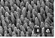 x 30 mm that have a needle-shaped surface structure where "needles" are made of single-crystal silicon and have a height above 10 µm (or more) and diameter about 1 µm maximum (see photo below). The quantity is 40 pieces (in this phase).
Reference #254222 for specs and pricing.
Black Silicon Surfaces for FLEXPOL Project
A university researcher requested a quote for the following.
We plan to use these wafer for developing black silicon surfaces for FLEXPOL project.
Item# 452: 100mm P(100) 1-100 ohm-cm 500um SSP Test Grade.
Reference #2018/1370 for specs and pricing.
One Inch Black Silicon Wafers For Optical Research
A project manager requested a quote for the following.
Do you sell silicon wafers, where one side is modified to provide a black silicon surface? I am interested in 100 mm wafers.
I would need ~5 pcs, the wafers could also be smaller, down to 1 inch would be ok. Square shaped would also be fine. The rest of the specs are not important, as they are intended to be used for the optical properties of the Black Silicon side.
Can you please also include the following items on the quote:
25x ID 590
25x ID 1617
Reference #267350 for specs and pricing.
Related Black Silicon Resources
Black Silicon to Fabricate Photodetector
A PhD candidate requested a quote for the following.
Do you carry any Black Silicon wafers? I don’t see any on your catalog.
In the original purchase, I would like to buy 100 pieces of 0.5” diameter black silicon. That would be the ideal case. I can work around whatever you would have available.
I'm looking for pieces (or a wafer) of black silicon to be built into a photodetector.
Black silicon is a textured silicon substrate that has a very high and constant absorption coefficient from the UV into the IR range. It’s built to have very little reflection, which is why it is called black silicon.
This is different from a flat Si wafer, which is typically gray. I know you guys supply these, I bought plenty when I was a graduate student.
Please let me know if you supply any black silicon as wafers or pieces.
Reference #204882 for specs and pricing.
Get Your Quote FAST! Or, Buy Online and Start Researching Today!
100mm Black Silicon Wafers
A PosDoc requested the following.
I am interested in purchasing 10-20 black silicon wafers. Silicon CZ prime grade, P Boron <100> 1-10 Ohm-cm, 100mm diameter x 500-550um thick with primary reference flat measuring 32.5mm +/- 2.5mm long and 1 secondary reference flat measuring 18mm +/- 2.0mm long, polished both sides, TTV <10um, bow <40um.
Reference #253709
Medical Devices Use Black Silicon Wafers
A startup requested a quote for the following.
We are an early stage startup company that deals with development of medical devices. We are looking for Black Silicon wafer pieces size 30 x 30 mm that have a needle-shaped surface structure where needles are made of single-crystal silicon and have a height above 10 µm or more and diameter about 1 µm maximum.
Reference #254222 for specs and pricing.
Black Silicon Surfaces for FLEXPOL Project
A university researcher requested a quote for the following.
We plan to use these wafers for developing black silicon surfaces for FLEXPOL project.
Item# 452: 100mm P(100) 1-100 ohm-cm 500um SSP Test Grade.
Reference #2018/1370 for specs and pricing.
One Inch Black Silicon Wafers For Optical Research
A project manager requested a quote for the following.
Do you sell silicon wafers, where one side is modified to provide a black silicon surface? I am interested in 100 mm wafers.
I would need ~5 pcs, the wafers could also be smaller, down to 1 inch would be ok. Square shaped would also be fine. The rest of the specs are not important, as they are intended to be used for the optical properties of the Black Silicon side.
Can you please also include the following items on the quote:
25x ID 590
25x ID 1617
Reference #267350 for specs and pricing.
What is Black Silicon?
Black silicon is a type of silicon material that has been modified to have a highly textured surface, which makes it appear black due to its increased light absorption. This is achieved by creating microscopic and nanoscopic structures on the silicon surface, often through processes like laser etching or plasma treatment. These structures trap light and reduce reflection, which is why black silicon has excellent anti-reflective properties.
Black silicon is particularly valuable in applications where enhanced light absorption is crucial, such as in solar cells, photodetectors, and other optical sensors. In solar technology, black silicon can help increase the efficiency of photovoltaic cells by capturing more sunlight and reducing the amount of light that is reflected away. This ability to trap light is beneficial for various fields, especially in environments where capturing as much light as possible is essential.
What Applications Use Black Silicon?
Black silicon's unique light-trapping and anti-reflective properties make it valuable in various applications, especially those involving light absorption and sensing. Here are some of the primary uses:
1. Solar Cells
- Enhanced Light Absorption: Black silicon's ability to absorb nearly all incident light makes it ideal for
 solar cells, as it maximizes the amount of sunlight converted to electricity.
- Improved Efficiency in Low-Light Conditions: Black silicon performs well in low-light or diffuse-light conditions, making it useful for solar installations in areas with varying sunlight.
2. Photodetectors and Optical Sensors
- Improved Sensitivity: Black silicon’s high surface area and light absorption enhance the sensitivity of photodetectors, allowing them to detect low-intensity light and improve device performance.
- Applications in LIDAR and Imaging: Black silicon sensors are effective in LIDAR technology for autonomous vehicles and in imaging devices for low-light environments, like night-vision cameras.
3. Medical and Biological Sensors
- Surface Area for Increased Sensitivity: Black silicon can be functionalized with biomolecules, making it useful in biosensing applications. Its large surface area and light-trapping abilities help in detecting very small quantities of biological substances.
- Non-Reflective Medical Imaging Surfaces: The material is also being explored for use in endoscopic and other imaging devices where reducing reflections can improve image clarity.
4. Infrared Detectors
- Better Infrared Absorption: Black silicon absorbs light across a wide spectrum, including infrared, making it suitable for infrared sensors used in thermal imaging, night vision, and environmental monitoring.
5. Anti-Reflective Coatings for Optical Devices
- Enhanced Performance in Optical Instruments: Its anti-reflective properties make it ideal for coatings in cameras, microscopes, and telescopes, helping reduce glare and increase the clarity of captured images.
6. Lab-on-a-Chip and Microfluidics Applications
- Enhanced Chemical Reactivity and Light Sensitivity: Black silicon is sometimes used in lab-on-a-chip devices, particularly those that require chemical reactions driven by light or a high surface area for improved sensitivity in biochemical assays.
7. Self-Cleaning Surfaces
- Hydrophobic Properties: Black silicon can be made hydrophobic, meaning it repels water. This is advantageous in creating self-cleaning surfaces for solar panels, windows, and other outdoor installations, reducing maintenance needs.
With ongoing research, black silicon’s applications continue to expand, especially in fields that benefit from its ability to trap light, increase surface reactivity, and reduce reflection.
What are the Most Common Specs of Black Silicon?
The specifications of black silicon can vary depending on the application and manufacturing process, but here are some common parameters and characteristics often specified for black silicon:
1. Wavelength Absorption Range
- Visible and Infrared Spectrum: Black silicon typically absorbs light over a broad range, including visible (400–700 nm) and near-infrared (up to around 1100 nm).
- Ultra-low Reflectance: Reflectance is often below 1% across the visible spectrum, maximizing light absorption.
2. Surface Morphology
- Nano-Needle Structures: Black silicon often has nano-sized needle-like structures or a forest of silicon spikes, with heights ranging from 100 nm to several micrometers, depending on the fabrication method.
- Feature Density: High-density structures, often exceeding 10^10 features per cm², enhance light trapping and absorption.
3. Sheet Resistance
- Range: Common sheet resistance values are between 1–50 Ω/, depending on doping levels.
- Customizable via Doping: Black silicon can be doped as n-type or p-type silicon to adjust conductivity, especially for electronic applications like photodetectors.
4. Reflectance Rate
- Ultra-low Reflectance: Black silicon typically exhibits a very low reflectance, often around 0.5% to 2%, making it highly effective at absorbing incident light.
- Directional Absorption: Surface morphology enables absorption from a wide range of incident angles, useful in applications where light hits the surface at different angles, such as solar cells.
5. Etch Depth
- Range: The etch depth, or depth of surface texturing, can vary from a few hundred nanometers to a few micrometers.
- Deeper Etches for Increased Absorption: Deeper etches are used in applications requiring maximum light absorption but can affect the structural stability of the surface.
6. Doping Type
- N-type or P-type Doping: Black silicon can be doped as n-type or p-type silicon, depending on the electronic application.
- Dopant Concentration: Doping levels are tailored to specific applications; for instance, solar cells may use lower dopant concentrations to avoid excessive charge recombination.
7. Hydrophobicity (Surface Wettability)
- Hydrophobic vs. Hydrophilic: Black silicon can be chemically modified to be either hydrophobic or hydrophilic.
- Self-Cleaning Surface Options: Hydrophobic black silicon is often used for self-cleaning surfaces, reducing the need for maintenance in outdoor applications.
8. Carrier Lifetime and Diffusion Length
- Typical Carrier Lifetimes: Black silicon typically has shorter carrier lifetimes than polished silicon due to the high surface area, which can lead to higher recombination rates. Specific treatments can improve carrier lifetimes for photovoltaic applications.
- Impact on Device Performance: For solar and photodetector applications, diffusion length and carrier lifetime need to be optimized to balance light absorption with efficient charge collection.
These specifications can be adjusted by different fabrication methods, such as reactive-ion etching, laser processing, or plasma treatment, to suit specific requirements in fields like photovoltaics, sensing, and optics.
