
Low Stress Silicon Nitride (SiN) Thin Films
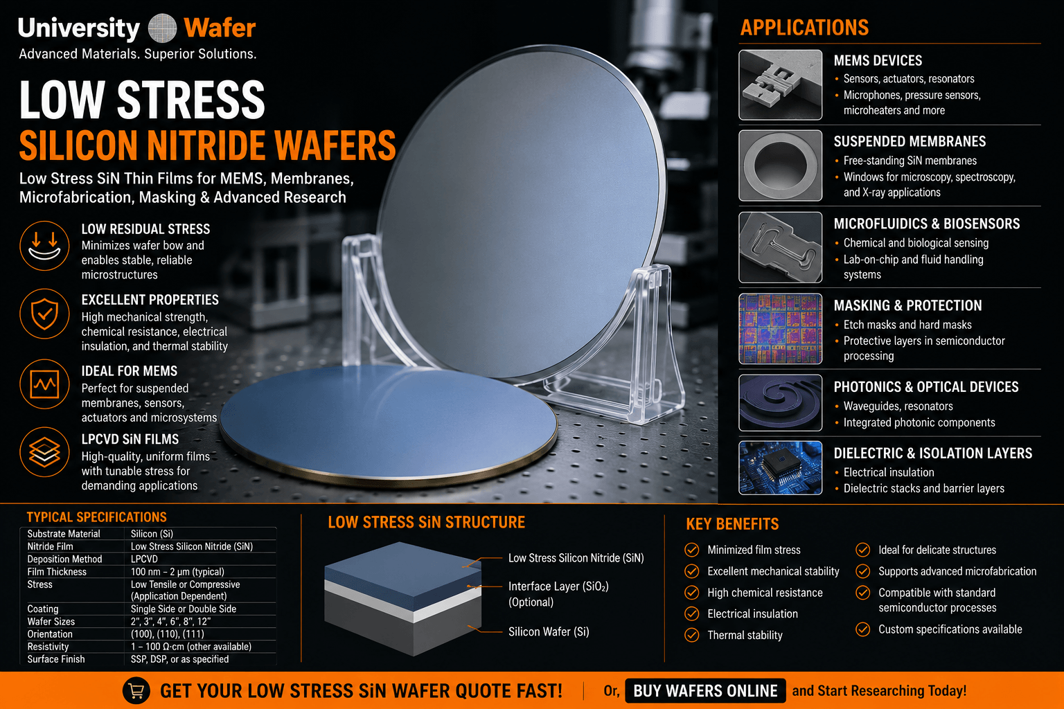
Low stress silicon nitride is a thin-film material engineered to reduce the internal mechanical stress normally associated with deposited silicon nitride. When deposited on silicon wafers, low stress SiN provides excellent mechanical strength, chemical resistance, electrical insulation, and thermal stability while reducing the risk of excessive wafer bow or deformation.
UniversityWafer supplies low stress silicon nitride wafers for universities, laboratories, semiconductor developers, and industrial R&D. These substrates are particularly useful for MEMS structures, suspended membranes, sensors, masking layers, and other applications where controlling film stress is critical.
Why Is Low Film Stress Important?
Mechanical stress within a deposited thin film can affect wafer flatness and the stability of microfabricated structures. Excessive tensile or compressive stress may cause thin structures to bend, deform, crack, or fail during fabrication.
Using a low stress nitride film helps minimize these effects, making the material particularly valuable for delicate suspended structures and precision microsystems.
- Reduced mechanical stress: Helps limit deformation in thin films and suspended structures.
- Excellent mechanical strength: Silicon nitride can form durable membranes and microstructures.
- Electrical insulation: Useful as a dielectric and isolation layer in semiconductor devices.
- Chemical resistance: Provides resistance to many chemicals used during microfabrication.
- Thermal stability: Suitable for semiconductor processes involving elevated temperatures.
- Barrier properties: SiN can function as a protective or diffusion-barrier layer in device structures.
LPCVD Low Stress Silicon Nitride
Low Pressure Chemical Vapor Deposition (LPCVD) is commonly used to deposit high-quality silicon nitride films onto silicon substrates. Process conditions and film composition can be adjusted to reduce residual stress while maintaining desirable mechanical and chemical properties.
LPCVD nitride films are valued for their uniformity and conformal coverage, making them useful for semiconductor processing and precision microfabrication. Film thickness and stress requirements should be selected according to the intended device and fabrication process.
Low Stress Nitride for MEMS
MEMS fabrication is one of the most important applications for low stress SiN. Thin nitride layers can serve as structural materials in microscopic sensors, actuators, resonators, and suspended components.
Reducing residual stress is especially important when fabricating free-standing structures because even small amounts of stress can affect their geometry and mechanical behavior. Researchers interested in related applications can explore silicon nitride for MEMS.
Silicon Nitride Membranes
Low stress SiN is widely used to fabricate thin suspended membranes and windows. A silicon substrate can be selectively etched beneath the nitride film, leaving a thin free-standing membrane supported by the surrounding wafer.
These structures are useful for microscopy, spectroscopy, sensors, microfluidics, nanotechnology, X-ray research, and other experiments requiring an extremely thin but mechanically stable supporting layer.
Masking & Microfabrication
Silicon nitride can also function as a masking and protective layer during semiconductor processing. Its chemical durability makes it useful in fabrication sequences involving selective etching and surface modification.
Depending on the process, researchers may combine silicon nitride with silicon dioxide layers to create dielectric stacks, masking structures, and specialized semiconductor devices.
Low Stress SiN for Sensors
The combination of mechanical strength, low residual stress, and electrical insulation makes low stress silicon nitride useful for sensor development. Thin SiN structures can be incorporated into pressure sensors, thermal sensors, resonators, biosensors, and other microfabricated devices.
Selecting Low Stress Nitride Wafers
The appropriate low stress silicon nitride wafer depends on the fabrication process and final device requirements. Important specifications may include:
- Silicon wafer diameter and thickness
- Crystal orientation
- Silicon conductivity and resistivity
- Silicon nitride film thickness
- Film stress requirements
- Single-side or double-side nitride coating
- Wafer surface finish
- Custom processing requirements
Researchers should consider both the properties of the underlying silicon substrate and the deposited SiN film when selecting wafers for MEMS, membrane, masking, or thin-film applications.
Get Your Low Stress Silicon Nitride Wafer Quote FAST! Or, Buy Wafers Online and Start Researching Today!
Low Stress Silicon Nitride Applications
Low stress silicon nitride (SiN) wafers are used in semiconductor and microfabrication processes where mechanical stability, chemical resistance, and precise thin-film performance are required. By minimizing residual film stress, SiN layers can support delicate structures that might otherwise bend, fracture, or deform during fabrication.
MEMS Devices & Microsystems
Low stress SiN is particularly valuable for MEMS device fabrication. Silicon nitride layers can function as structural, insulating, protective, or masking materials within microscopic devices.
Applications can include:
- Pressure sensors
- Microphones and acoustic devices
- Microheaters
- Resonators
- Micro-actuators
- Thermal sensors
- Microfluidic devices
- Suspended MEMS structures
Researchers working specifically with microsystems can also explore silicon nitride wafers for MEMS.
Free-Standing SiN Membranes
One of the most important applications of low stress nitride is the fabrication of free-standing silicon nitride membranes. Selected regions of the underlying silicon can be removed through microfabrication processes, leaving an extremely thin SiN membrane suspended across an opening.
Controlling residual stress is especially important for these structures because excessive stress can cause membrane deformation or mechanical failure. Low stress films help maintain flatter, more stable membranes for precision research.
Microscopy & Electron-Beam Research
Thin silicon nitride membranes can provide supporting windows for electron microscopy, X-ray analysis, spectroscopy, and nanomaterial characterization. Their combination of low thickness and mechanical strength allows researchers to support microscopic samples while minimizing the amount of substrate material interacting with the measurement.
Microfluidics & Biosensors
Low stress SiN can be incorporated into microfluidic devices and biosensors as a structural membrane, dielectric layer, passivation layer, or interface between different regions of a device.
These properties make silicon nitride useful for research involving lab-on-a-chip systems, biological sensing, chemical detection, fluid handling, and other miniaturized analytical devices.
Dielectric & Electrical Isolation Layers
Silicon nitride is an electrical insulator and can function as a dielectric layer within semiconductor structures. It may be used to electrically isolate conductive components, protect underlying materials, or form part of multilayer device architectures.
Depending on the application, SiN may be combined with thermal silicon dioxide to create dielectric stacks with specific electrical, optical, or processing characteristics.
Etch Masks & Protective Layers
The chemical resistance of silicon nitride makes it useful as an etch mask and protective film during semiconductor fabrication. SiN layers can protect selected regions of a silicon substrate while other areas undergo etching or surface processing.
This capability is particularly valuable when fabricating cavities, membranes, channels, and other three-dimensional structures in silicon wafers.
Thin-Film & Nanotechnology Research
Low stress silicon nitride wafers are also used as platforms for thin-film deposition, nanofabrication, and materials characterization. Researchers can deposit metals, semiconductor layers, nanomaterials, or functional coatings onto the SiN surface to investigate electrical, mechanical, optical, and chemical properties.
Photonics & Optical Devices
Silicon nitride is also an important material for integrated photonics. Carefully engineered SiN layers can be patterned into optical structures such as waveguides, resonators, and other components used to manipulate light on a chip.
Film thickness, refractive index, surface quality, and stress must be carefully controlled for demanding photonic applications.
Single-Side vs. Double-Side Nitride
Low stress nitride coatings may be required on one or both sides of a silicon wafer. Single-side coatings can be appropriate when only one device surface requires SiN, while double-side coatings can be useful for masking, membrane fabrication, or processes where both wafer surfaces participate in fabrication.
The appropriate configuration depends on the lithography, etching, deposition, bonding, and device-processing sequence.
Important Wafer & Film Specifications
When ordering low stress silicon nitride wafers, researchers should define the specifications that affect their fabrication process. These may include:
- Wafer diameter
- Silicon wafer thickness
- Crystal orientation
- Resistivity and conductivity type
- SiN film thickness
- Film stress
- Single-side or double-side coating
- Surface finish
- Wafer flatness and TTV requirements
- Quantity and custom processing requirements
Research & Production Applications
From MEMS membranes and sensors to microfluidics, photonics, dielectric structures, and nanotechnology, low stress silicon nitride provides a versatile thin-film platform for both experimental research and semiconductor device development.