
Silicon Wafers for Research and Development
Silicon wafers are the foundation of modern semiconductor technology and are widely used in university laboratories, industrial R&D, and device fabrication. Their well-established electrical, mechanical, and thermal properties make silicon an excellent substrate for a broad range of experimental applications.
Why Use Silicon Wafers?
Silicon substrates provide a reliable platform for semiconductor processing, thin-film deposition, lithography, oxidation, and device fabrication. Researchers can select wafer specifications to match the requirements of their particular process.
- Semiconductor fabrication and integrated circuits
- MEMS (Microelectromechanical Systems)
- Sensors and microelectronic devices
- Thin-film deposition and coating research
- Photovoltaic and solar-cell research
- Lithography and process-development experiments
- Materials characterization and academic research
Silicon Wafer Crystal Orientation
Common silicon wafer orientations include <100> and <111>. Crystal orientation can influence etching behavior, oxidation, epitaxial growth, and device processing, making it an important specification when choosing a wafer.
Prime, Test and Research-Grade Wafers
Different applications require different wafer grades. Prime-grade silicon wafers are typically selected for demanding fabrication and research processes, while test and research-grade wafers can provide economical substrates for equipment testing, deposition trials, process development, and teaching laboratories.
Choose the Right Silicon Wafer
Important specifications include diameter, thickness, orientation, dopant type, resistivity, surface finish, and wafer grade. Silicon wafers may be supplied as P-type or N-type substrates and with polished surfaces appropriate for a variety of research processes.
UniversityWafer can help researchers identify silicon substrates suited to semiconductor processing, MEMS, optics, materials science, and other R&D applications.
Get Your Silicon Wafer Quote FAST! Or Buy Online and Start Researching Today!
Silicon Wafer Properties and Applications
Silicon (Si) wafers are widely used as substrates for semiconductor fabrication and scientific research. Their excellent electrical properties, mechanical stability, thermal performance, and compatibility with established fabrication processes make silicon a versatile material for electronics, MEMS, sensors, photonics, and thin-film research.
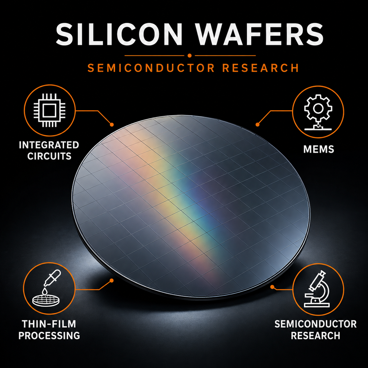
Common Silicon Wafer Applications
- Integrated circuits (ICs) and microelectronics
- MEMS (Microelectromechanical Systems)
- Sensors and semiconductor devices
- Thin-film deposition and coating development
- Thermal oxidation and dielectric research
- Photolithography and process development
- Solar cells and photovoltaic research
- Photonics and optical device research
P-Type and N-Type Silicon Wafers
Silicon wafers can be produced with different conductivity types. P-type silicon is commonly doped with acceptor elements such as boron, while N-type silicon commonly uses donor dopants such as phosphorus. The appropriate conductivity type and resistivity depend on the intended device or experiment.
Silicon Wafer Surface Finishes
Researchers can select single-side polished (SSP) or double-side polished (DSP) silicon wafers depending on their application. DSP wafers are useful when high-quality surfaces are required on both sides, while SSP wafers are suitable for many standard semiconductor and materials-research processes.
Silicon Wafers for MEMS
Silicon's mechanical properties and compatibility with established microfabrication techniques make it an important material for MEMS devices. Applications include pressure sensors, accelerometers, microfluidic structures, resonators, and other microscale devices.
Silicon for Thin-Film and Process Research
Silicon substrates provide a well-characterized surface for thin-film deposition, ALD, CVD, PVD, oxidation, etching, and lithography. They can be used to evaluate new materials, coatings, fabrication processes, and semiconductor equipment.
Silicon Wafer Specifications
When selecting a silicon wafer, consider diameter, thickness, crystal orientation, dopant, conductivity type, resistivity, surface finish, and wafer grade. Matching these specifications to your research process can help improve experimental consistency and device performance.