
Why Is Silicon Wafer Cleaning Important?
Proper silicon wafer cleaning helps control particles, organic residues, metallic contamination, and unwanted surface films before semiconductor processing. Surface contamination can interfere with lithography, deposition, bonding, epitaxy, electrical characterization, and other fabrication steps where surface condition is critical.
The goal is not simply to make a wafer “clean,” but to prepare the surface for the process that follows. Different applications may require different surface conditions, so the cleaning method should be selected according to the wafer, existing films, contamination type, and next fabrication step.
Surface Preparation Before Semiconductor Processing
Silicon wafers may require surface preparation before processes such as photolithography , thin-film deposition , oxidation, epitaxial growth , wafer bonding, MEMS fabrication, and surface analysis.
Common surface-preparation goals include removing:
- Particles and handling debris
- Photoresist and organic residues
- Oils and processing contamination
- Metallic and ionic contaminants
- Native oxide when an oxide-free silicon surface is required
Choosing the Correct Wafer Cleaning Method
There is no single cleaning chemistry that is appropriate for every silicon wafer. A suitable process should be chosen based on the material already present on the wafer and the surface required afterward.
- Solvent cleaning can be useful for many organic residues, oils, and photoresist-related contamination.
- RCA cleaning is widely used for particle, organic, and metallic contamination control.
- Piranha cleaning is a strong oxidizing treatment used for persistent organic contamination on compatible samples.
- HF-based cleaning is used when silicon dioxide or native oxide must be removed before a subsequent process.
Researchers should consider chemical compatibility carefully, especially when the wafer contains patterned structures, deposited films, metals, polymers, or other materials that may be affected by aggressive cleaning chemistry.
Silicon Wafer Specifications That Affect Cleaning
The starting wafer can influence how a cleaning process is developed and evaluated. Important specifications may include:
- Wafer diameter: affects handling, carriers, equipment, and process compatibility.
- Crystal orientation: such as <100> or <111>, depending on the fabrication process.
- Dopant and resistivity: important for electrical and device research.
- Surface finish: single-side polished, double-side polished, or other surface preparation.
- Existing oxide: thermal oxide or native oxide may be intentionally retained or removed.
- Deposited films: metals, nitrides, dielectrics, photoresists, and other coatings may limit which cleaning chemistries can be used.
- Wafer grade: prime, test, mechanical, reclaimed, or other grades may be selected according to the experiment and required surface quality.
Silicon Wafers for Cleaning and Process Development
UniversityWafer supplies silicon wafers for semiconductor fabrication, cleaning studies, surface preparation, MEMS, photonics, thin-film research, wafer bonding, and university laboratories.
Available specifications can include different wafer diameters, thicknesses, crystal orientations, dopants, resistivity ranges, surface finishes, oxide layers, and custom configurations for research and process-development requirements.
Need Silicon Wafers for Cleaning, Surface Preparation, or Semiconductor Research? Or, Buy Online and Start Researching Today!
Common Research Applications
Clean and well-characterized silicon surfaces are used in a wide range of semiconductor and materials research applications, including:
- Semiconductor process development
- MEMS fabrication
- Photolithography experiments
- Thin-film deposition studies
- Wafer bonding research
- Epitaxial growth
- Surface characterization
- Oxidation and diffusion studies
- Photonics and optical devices
- University laboratory experiments
Silicon Wafer Cleaning Process
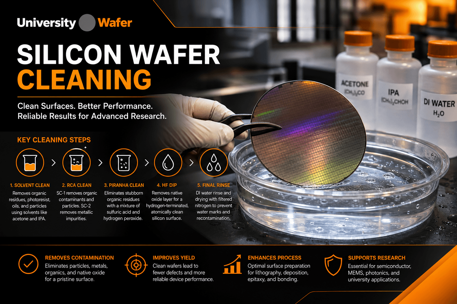
A silicon wafer cleaning process is designed to remove unwanted particles, organic residues, metallic contamination, and other surface contaminants before semiconductor processing or materials research. The appropriate cleaning sequence depends on the wafer condition, the contaminants present, and the fabrication step that follows.
Wafer cleaning may be performed before photolithography, thin-film deposition, oxidation, wafer bonding, surface characterization, and epitaxial growth. Because different cleaning chemistries target different contaminants, there is no single cleaning sequence that is appropriate for every application.
Common Silicon Wafer Cleaning Methods
Semiconductor laboratories use several chemical and physical cleaning methods. The method should be selected according to the type of contamination and the surface condition required for the next process step.
| Cleaning Method | Primary Purpose | Common Application |
|---|---|---|
| Solvent Cleaning | Removes many organic residues, oils, grease, and some photoresist residues | Initial surface preparation before additional wafer cleaning |
| RCA SC-1 | Helps remove particles and organic contamination | General silicon wafer surface cleaning |
| RCA SC-2 | Helps remove metallic and ionic contamination | Surface preparation where trace-metal contamination is a concern |
| Piranha Cleaning | Strong oxidation and removal of organic contamination | Removal of persistent organic residues when compatible with the sample and process |
| HF Treatment | Removes silicon dioxide, including native oxide | Surface preparation when oxide removal is required before a subsequent process |
What Contaminants Are Removed During Wafer Cleaning?
Silicon wafers can acquire contamination during handling, storage, lithography, deposition, etching, polishing, and other processing steps. Common contaminants include:
- Particles: Dust, process debris, and other particles can interfere with lithography, deposition, bonding, and patterned device structures.
- Organic residues: Photoresist residues, oils, fingerprints, polymers, and other carbon-containing contaminants may remain on the wafer surface.
- Metallic contamination: Trace metals can affect semiconductor electrical properties and interfere with sensitive fabrication processes.
- Ionic contamination: Mobile ionic species can be undesirable in semiconductor structures and dielectric layers.
- Native oxide: Silicon exposed to air naturally develops a thin surface oxide. Some processes require this oxide to remain, while others require its removal immediately before processing.
RCA Wafer Cleaning
RCA cleaning is a widely used wet-chemical procedure for preparing silicon wafer surfaces. The traditional process uses separate cleaning stages because particle and organic contamination require different chemistry from metallic contamination.
SC-1 Cleaning
Standard Clean 1 (SC-1) typically uses ammonium hydroxide (NH4OH), hydrogen peroxide (H2O2), and deionized water. It is primarily used to help remove particles and organic contamination from silicon surfaces.
SC-2 Cleaning
Standard Clean 2 (SC-2) typically uses hydrochloric acid (HCl), hydrogen peroxide (H2O2), and deionized water. This stage is primarily used to reduce metallic contamination.
RCA procedures can be modified according to the substrate, contamination level, equipment, and subsequent process. Researchers should therefore follow a validated laboratory or fabrication protocol rather than assuming that one RCA sequence is appropriate for every wafer.
Piranha Cleaning for Silicon Wafers
Piranha cleaning uses sulfuric acid and hydrogen peroxide and is a powerful oxidizing treatment for removing organic contamination. It can be useful when persistent organic residues must be removed from compatible surfaces.
Piranha solution is highly reactive and can react dangerously with incompatible materials. It should only be used under an established laboratory safety protocol with appropriate equipment, training, and chemical-handling controls.
HF Cleaning and Native Oxide Removal
Hydrofluoric-acid-based treatments are used when a process requires removal of silicon dioxide from a silicon surface. This can include the thin native oxide that develops after silicon is exposed to air.
After appropriate HF treatment, the silicon surface can become hydrogen-terminated and comparatively hydrophobic. The surface can subsequently change again after exposure to air or processing environments, so timing and handling after oxide removal can be important for applications such as epitaxy, bonding, and selected deposition processes.
Wafer Cleaning Before Thin-Film Deposition
Surface preparation can strongly influence deposited-film adhesion, uniformity, interfaces, and reproducibility. Before thin-film deposition , researchers may need to remove particles, organic residues, metals, or surface oxide depending on the film material and deposition process.
The desired starting surface is process-dependent. For example, some experiments require oxide-free silicon, while others intentionally use a thermally oxidized or otherwise coated silicon substrate.
Wafer Cleaning Before Photolithography
Clean and appropriately prepared wafer surfaces are important for photolithography . Particles and organic contamination can interfere with resist coating, pattern formation, adhesion, and subsequent processing.
Surface preparation should be matched to the photoresist system and fabrication process rather than applying an aggressive chemical clean automatically.
Best Practices for Silicon Wafer Surface Preparation
A reliable wafer-cleaning procedure should be selected according to the substrate, contamination type, and next fabrication step. General process considerations include:
- Identify the contaminants that actually need to be removed.
- Use chemicals and cleaning methods compatible with the wafer and existing films.
- Use high-purity reagents and appropriate deionized-water rinsing when required.
- Minimize unnecessary wafer handling after cleaning.
- Use clean containers, tools, and controlled processing environments.
- Avoid introducing particles or metals during handling and drying.
- Consider how quickly the surface may change after oxide removal or other treatments.
- Use a validated process when cleaning wafers for sensitive fabrication steps.
Applications That Require Controlled Wafer Cleaning
Silicon surface preparation is used throughout semiconductor research and fabrication, including:
- Semiconductor device fabrication
- MEMS and microsystem fabrication
- Photonic and optical device research
- Photolithography
- Thin-film deposition
- Epitaxial growth
- Wafer bonding
- Oxidation and diffusion processes
- Surface characterization and metrology
- Solar-cell and photovoltaic research
- University and industrial laboratory research
Choosing Silicon Wafers for Cleaning and Process Research
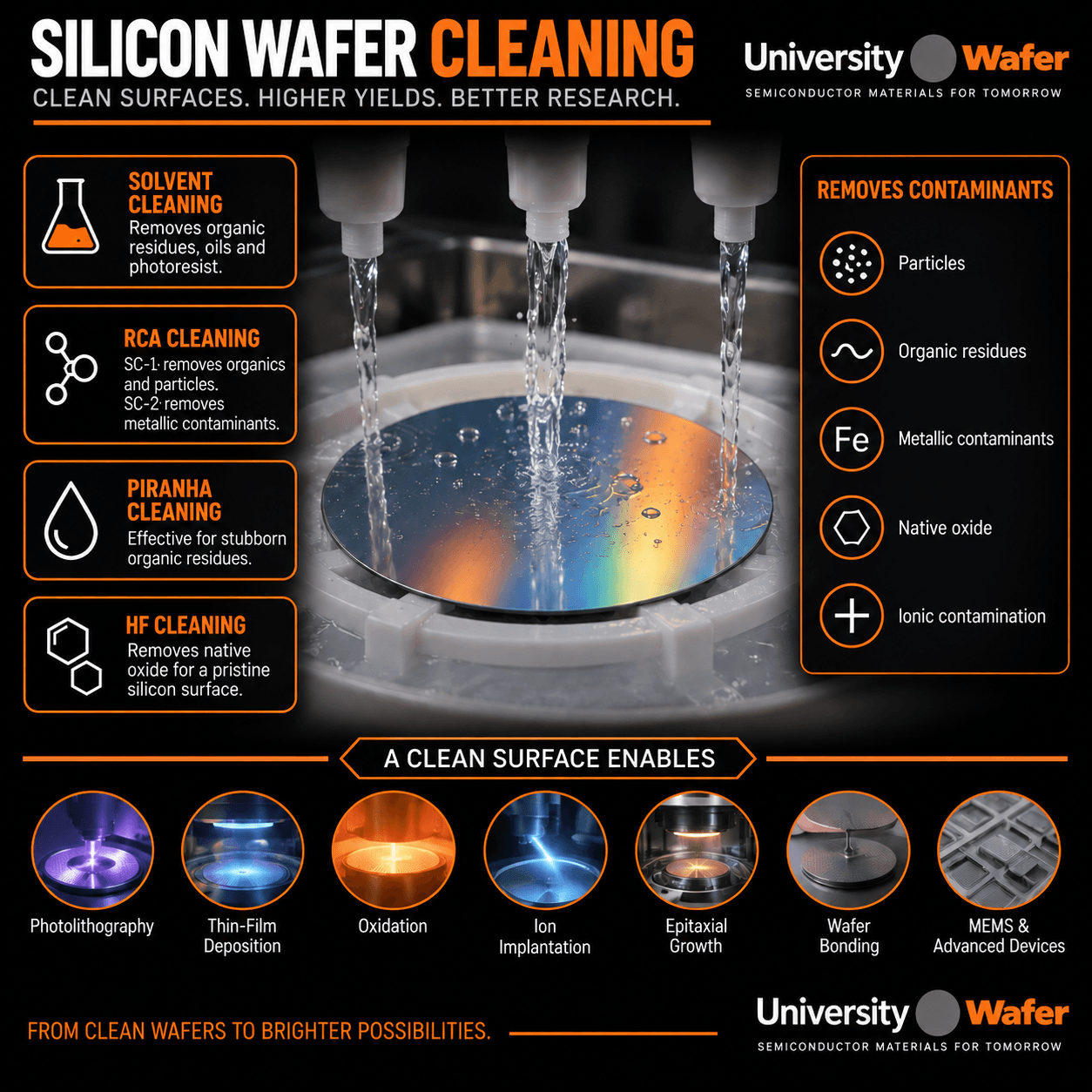
The starting wafer can be just as important as the cleaning process. Researchers should consider specifications such as diameter, thickness, crystal orientation, dopant, conductivity type, resistivity, surface finish, TTV, and existing oxide or deposited films when selecting silicon substrates for process-development experiments.
UniversityWafer supplies silicon wafers for semiconductor fabrication, MEMS, photonics, thin-film research, surface studies, and university laboratories. Available configurations include prime, test, mechanical, oxidized, SOI, and custom silicon substrates for a wide range of research and process-development requirements.