
Why Choose Reclaimed Silicon Wafers?
Reclaimed silicon wafers offer a practical and economical solution for applications where a brand-new prime wafer is not required. Previously used wafers are professionally stripped, cleaned, inspected, and repolished to restore their surface, making them suitable for equipment qualification, process development, thin-film deposition, and cleanroom training. By reusing high-quality substrates, laboratories and manufacturers can significantly reduce material costs without compromising process evaluation.
UniversityWafer supplies silicon wafers that have been reclaimed to meet demanding research and manufacturing requirements. Our reclaimed substrates are available in a variety of diameters, crystal orientations, thicknesses, and surface finishes, providing an excellent choice for universities, government laboratories, and commercial semiconductor fabrication facilities.
Common Applications
- Carrier wafers for semiconductor processing
- Dummy wafers for equipment qualification
- Monitor wafers for process evaluation
- Thin-film deposition and coating development
- Photolithography process optimization
- Etching, cleaning, and CMP process testing
- MEMS and sensor process development
- University teaching laboratories and cleanroom training
- Equipment calibration and maintenance
- Prototype manufacturing and R&D
Available Options
Our reclaimed silicon wafers are available in multiple diameters, including 2-inch through 300 mm, with <100>, <111>, and other crystal orientations. Options include single-side polished (SSP), double-side polished (DSP), various thicknesses, resistivities, and custom specifications to match your semiconductor process requirements.
Get Your Reclaimed Silicon Wafer Quote FAST!
Whether you need reclaimed wafers for equipment testing, process development, or cleanroom training, our specialists can help you select the right substrate for your application while minimizing material costs.
Get Your Reclaimed Silicon Wafer Quote FAST! Or Buy Online and Start Researching Today!
What Are Reclaimed Silicon Wafers?
Reclaimed silicon wafers are previously used silicon substrates that have undergone a carefully controlled reclaim process to restore their surface quality for reuse. During reclamation, existing films and contaminants are removed through stripping, chemical cleaning, polishing, and final inspection. The result is a cost-effective wafer suitable for many semiconductor processes where a brand-new prime wafer is not necessary. Reclaimed wafers help manufacturers reduce material costs while supporting sustainable semiconductor manufacturing practices.
Unlike prime-grade silicon wafers, reclaimed wafers are generally used for equipment qualification, process monitoring, deposition trials, and other non-device applications. They provide excellent value for process development while maintaining the dimensional characteristics required for modern semiconductor fabrication equipment.
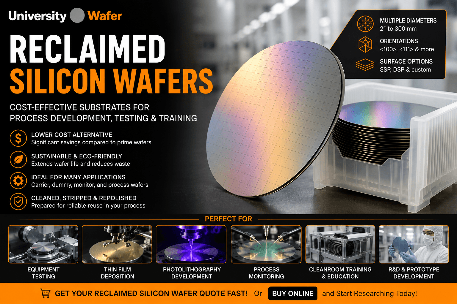
Benefits of Reclaimed Silicon Wafers
- Significantly lower cost than new prime-grade wafers
- Environmentally friendly by extending wafer life and reducing waste
- Excellent for equipment qualification and preventive maintenance
- Ideal for process development and engineering trials
- Compatible with deposition, lithography, etching, and CMP processes
- Available in a wide range of diameters, orientations, and thicknesses
- Suitable for universities, research labs, and semiconductor manufacturers
Typical Applications
Reclaimed silicon wafers are commonly used as carrier wafers, dummy wafers, monitor wafers, and process wafers throughout semiconductor manufacturing. They are frequently utilized for thin-film deposition, photolithography setup, plasma etching, oxidation studies, chemical mechanical polishing (CMP), cleanroom training, equipment calibration, and process optimization before transitioning to higher-value production wafers. Their affordability makes them an excellent choice for high-volume engineering work and academic research.
Selecting the Right Reclaimed Wafer
When choosing reclaimed silicon wafers, important considerations include wafer diameter, crystal orientation, resistivity, thickness, surface finish, flatness, and the intended manufacturing process. UniversityWafer supplies reclaimed wafers in multiple specifications to meet the needs of semiconductor process engineers, MEMS researchers, photonics laboratories, and educational institutions seeking reliable substrates at a lower cost than prime-grade wafers.