
Silicon Nitride Wafers for MEMS Research
Silicon nitride (Si3N4) is widely used in MEMS (Micro-Electro-Mechanical Systems) because it combines mechanical strength, chemical resistance, electrical insulation, and compatibility with established silicon microfabrication processes.
UniversityWafer supplies silicon nitride wafers for university laboratories, semiconductor R&D, sensor development, microfluidics, and experimental MEMS fabrication.
Why Use Silicon Nitride in MEMS?
MEMS structures often require thin films capable of maintaining mechanical stability after deposition, patterning, and etching. Silicon nitride can provide a durable structural or dielectric layer while also functioning as an effective mask during selected silicon processing steps.
- Excellent mechanical strength
- Good chemical resistance
- Electrical insulation
- Useful barrier and passivation properties
- Compatibility with silicon microfabrication
- Available with controlled film stress
- Useful as an etch-mask material
Low-Stress Silicon Nitride for MEMS
Film stress is an important consideration when fabricating suspended MEMS structures. Excessive tensile or compressive stress can cause thin membranes, cantilevers, and other structures to deform or fail.
Low-stress silicon nitride is therefore commonly selected for MEMS experiments involving freestanding structures, thin membranes, micromechanical components, and other stress-sensitive devices.
LPCVD Silicon Nitride
LPCVD (Low-Pressure Chemical Vapor Deposition) silicon nitride is frequently used when researchers require dense, uniform nitride films with strong mechanical and dielectric properties.
LPCVD nitride is especially useful for MEMS membranes, masking layers, dielectric structures, and microfabrication processes where film quality and thickness uniformity are important.
PECVD Silicon Nitride
PECVD (Plasma-Enhanced Chemical Vapor Deposition) provides another method for depositing silicon nitride. Its lower deposition temperature can be beneficial when a process includes materials or device structures that cannot tolerate the higher temperatures associated with conventional LPCVD processing.
Researchers should select LPCVD or PECVD films according to their desired film stress, deposition temperature, composition, electrical properties, and overall fabrication sequence.
Silicon Nitride MEMS Applications
- MEMS membranes and diaphragms
- Pressure sensors
- Cantilevers and micromechanical structures
- Microfluidic devices
- Dielectric layers
- Passivation and barrier layers
- Etch masks for silicon processing
- Optical MEMS
- Biosensors and research devices
Silicon Nitride for KOH Etching
Silicon nitride is commonly investigated as a masking material during anisotropic silicon etching processes such as KOH (potassium hydroxide) etching. Patterned nitride layers can protect selected regions of the silicon surface while exposed areas are etched to form cavities, membranes, channels, and other MEMS structures.
Choosing a Silicon Nitride MEMS Wafer
Important specifications depend on the fabrication process and device design. Researchers may need to specify:
- Wafer diameter and thickness
- Silicon crystal orientation
- Nitride film thickness
- LPCVD or PECVD deposition
- Stoichiometric or low-stress nitride
- Film stress requirements
- Single-side or double-side coating
- Surface finish and resistivity
Need Silicon Nitride Wafers for Your MEMS Project?
Send UniversityWafer your required wafer diameter, silicon orientation, nitride thickness, deposition method, film stress, coating configuration, and other process requirements. We can help identify an appropriate Si3N4-on-silicon wafer for your MEMS research.
Get Your Silicon Nitride MEMS Wafer Quote FAST! Or Buy Online and Start Researching Today!
How Is Silicon Nitride Used in MEMS?
Silicon nitride (Si3N4) is an important thin-film material in MEMS fabrication because it can serve several functions within the same device. Depending on the process, silicon nitride may act as a structural membrane, dielectric, passivation layer, diffusion barrier, or etch mask.
When deposited on silicon wafers, carefully controlled Si3N4 films can support the fabrication of microstructures ranging from pressure-sensitive membranes to suspended mechanical components.
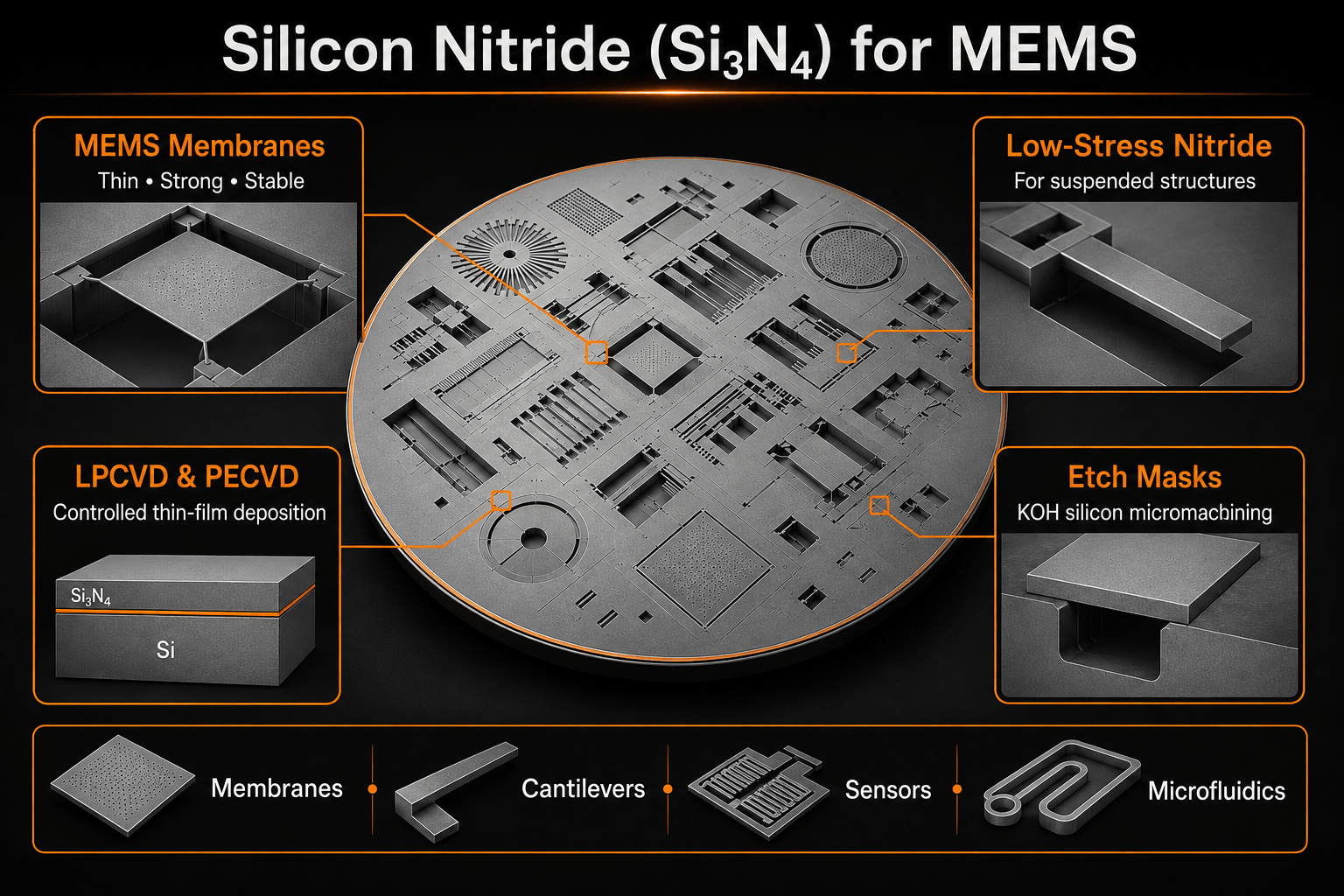
Silicon Nitride MEMS Membranes
Thin silicon nitride membranes are used in many MEMS and sensor research applications. Their combination of mechanical strength and small thickness allows researchers to fabricate suspended structures that interact with pressure, mechanical forces, fluids, light, or other environmental changes.
Research applications can include:
- Pressure-sensing diaphragms
- Thin-film membranes
- Microphones and acoustic devices
- Thermal sensors
- Microfluidic structures
- Optical MEMS
- Biosensor platforms
Film Stress in MEMS Fabrication
Controlling silicon nitride film stress is particularly important for suspended MEMS structures. Excessive stress can influence membrane flatness, dimensional stability, device sensitivity, and the mechanical behavior of fabricated structures.
For this reason, low-stress silicon nitride is often selected for membranes, cantilevers, bridges, and other micromechanical structures where deformation must be minimized.
LPCVD vs. PECVD Nitride for MEMS
Both LPCVD and PECVD processes can produce silicon nitride films, but the appropriate choice depends on the fabrication sequence, temperature budget, mechanical requirements, and desired film properties.
| Property | LPCVD Nitride | PECVD Nitride |
|---|---|---|
| Deposition Method | Low-Pressure Chemical Vapor Deposition | Plasma-Enhanced Chemical Vapor Deposition |
| Typical Process Temperature | Higher | Lower |
| Film Density | Generally high | Process dependent |
| Film Stress | Can be engineered for low-stress applications | Can be adjusted through deposition conditions |
| Common MEMS Uses | Membranes, structural layers, etch masks | Passivation, dielectric layers, lower-temperature processing |
Si3N4 as a Silicon Etch Mask
Silicon nitride's resistance to certain chemical processes makes it useful as a masking layer during silicon micromachining. Patterning the nitride can expose selected areas of the underlying silicon while protecting other regions during etching.
This approach is commonly associated with anisotropic wet etching using KOH (potassium hydroxide), which can be used to create cavities, trenches, diaphragms, and other three-dimensional structures in silicon.
Silicon Nitride for MEMS Sensors
MEMS sensors convert physical or environmental changes into measurable signals. Silicon nitride films may form part of the mechanical structure, electrical isolation system, protective coating, or sensing interface of these devices.
- Pressure sensors
- Gas and chemical sensors
- Thermal sensors
- Biomedical sensors
- Microcantilever sensors
- Optical sensing devices
Other Silicon Nitride Microfabrication Applications
Beyond conventional MEMS devices, Si3N4 wafers are used across semiconductor research, microfluidics, silicon photonics, biosensing, and experimental nanofabrication.
Researchers may also investigate silicon nitride for thin-film resonators, suspended nanostructures, dielectric isolation, protective coatings, and interfaces between electronic, mechanical, optical, and biological systems.
Silicon Nitride MEMS Research
UniversityWafer supplies silicon nitride coated substrates for proof-of-concept experiments, university research, process development, material characterization, and prototype MEMS fabrication. Selecting the appropriate film thickness, deposition method, stress level, and silicon substrate can help researchers match the starting wafer to their fabrication process.