Silicon Wafers for Semiconductor, MEMS & Photonics Research
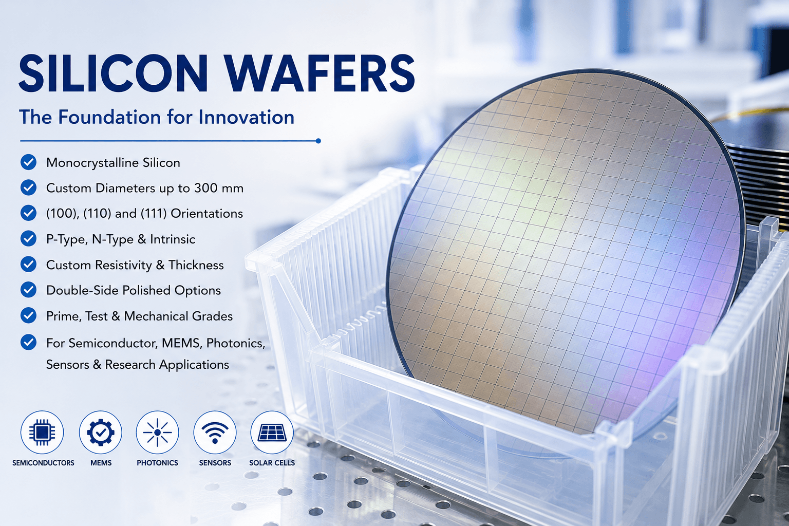
UniversityWafer supplies high-quality monocrystalline silicon wafers for semiconductor fabrication, MEMS, photonics, power electronics, microfluidics, sensors, and university research. Choose from standard or custom wafer diameters, crystal orientations, conductivity types, dopants, resistivities, thicknesses, and polished surface finishes to meet your exact device fabrication requirements.
Need Custom Silicon Wafers for Your Research?
UniversityWafer supplies high-quality monocrystalline silicon wafers
for semiconductor fabrication, MEMS, photonics, microelectronics, sensors, solar
cells, and university research. Whether you need standard substrates or custom
specifications, our engineering team can help you select the ideal wafer for your
process.
Recent Research Inquiry
"Our research group is fabricating MEMS pressure sensors and requires
100 mm <100> p-type silicon wafers with a resistivity of
1–10 Ω·cm, 525 µm thickness, double-side polished surfaces, and
prime-grade quality. Please provide pricing, lead time, and available
quantities for prototype fabrication."
Custom Silicon Wafer Options
- 1" to 12" (25 mm–300 mm) wafer diameters
- <100>, <110>, and <111> crystal orientations
- P-type, N-type, intrinsic, and heavily doped silicon
- Boron, phosphorus, arsenic, and antimony dopants
- Custom resistivity and wafer thickness
- Single-side polished (SSP) and double-side polished (DSP)
- Prime, test, reclaimed, and mechanical grades
- Fast quotations for research and production quantities
Complete the form below with your desired wafer diameter, orientation,
conductivity type, resistivity, thickness, surface finish, quantity,
and any special processing requirements. Our engineers will recommend
the best silicon wafer for your application and provide
a fast quotation.
Get Your Silicon Wafer Quote FAST! Or Buy Online and Start Researching Today!
Why Silicon Wafers Are the Foundation of Modern Electronics
Silicon wafers are the most widely used substrates in the semiconductor industry,
providing the foundation for integrated circuits, MEMS devices, power electronics,
photonic components, sensors, and solar cells. Their excellent electrical properties,
mechanical strength, thermal stability, and abundance make monocrystalline silicon
the preferred material for research, prototype development, and high-volume manufacturing.
How Silicon Wafers Are Manufactured
High-purity silicon is refined and grown into a single-crystal ingot using the
Czochralski (CZ) or Float Zone (FZ) process. The ingot is then sliced into thin
wafers, lapped, chemically etched, polished, and thoroughly cleaned to produce
substrates with exceptional flatness and low surface roughness. Depending on the
application, wafers may be supplied as prime, test, reclaimed, or mechanical grade.
Available Silicon Wafer Specifications
- Diameters from 25 mm to 300 mm (1"–12")
- Crystal orientations including <100>, <110>, and <111>
- P-type, N-type, intrinsic, and heavily doped substrates
- Boron, phosphorus, arsenic, or antimony doping
- Custom resistivity and wafer thickness
- Single-side polished (SSP) or double-side polished (DSP)
- Prime, test, reclaimed, and mechanical grades
- Custom flats or notches to SEMI standards
Common Research and Industrial Applications
Silicon wafers are used throughout semiconductor fabrication for CMOS integrated
circuits, MEMS sensors, RF devices, photonic integrated circuits, microfluidic
devices, biosensors, wafer bonding, thin-film deposition, oxidation studies,
lithography process development, and advanced packaging. They are also widely used
in university laboratories for materials science, nanotechnology, and device
characterization.
Choosing the Right Silicon Wafer
Selecting the proper silicon wafer depends on your fabrication process and device
requirements. Important considerations include crystal orientation, conductivity
type, resistivity, thickness, surface finish, wafer diameter, dopant species,
and whether the substrate requires thermal oxide, epitaxial silicon, silicon
nitride, or other deposited films. UniversityWafer supplies custom silicon wafers
manufactured to meet both research and production specifications.
