
Silicon Nitride Wafers for Advanced Research
UniversityWafer supplies silicon nitride (Si3N4) coated wafers for researchers working in MEMS, semiconductor fabrication, sensors, microelectronics, photonics, and thin-film development. Silicon nitride films provide useful electrical insulation, chemical resistance, mechanical strength, and barrier properties for a wide range of experimental processes.
LPCVD and PECVD Silicon Nitride
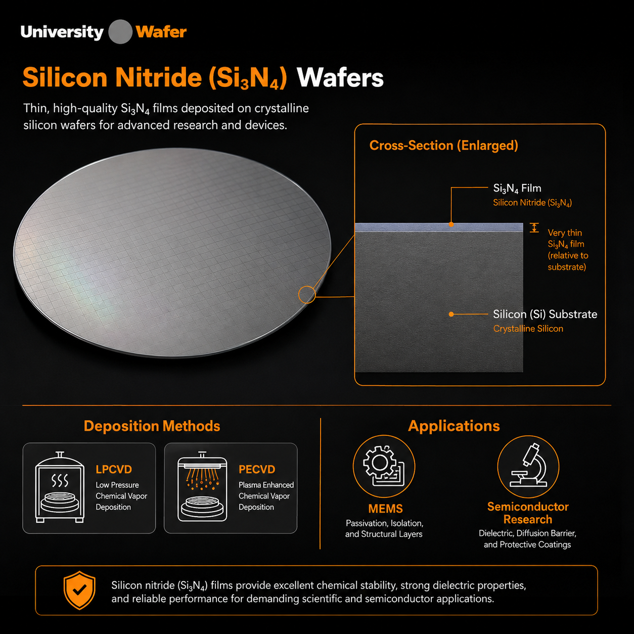
The deposition method can be selected according to the requirements of the research. LPCVD (Low-Pressure Chemical Vapor Deposition) is commonly used when researchers need dense, uniform silicon nitride films, while PECVD (Plasma-Enhanced Chemical Vapor Deposition) enables deposition at lower processing temperatures.
Silicon Nitride Film Options
Depending on your application, silicon nitride coated wafers may be specified with different film characteristics, including:
- Stoichiometric silicon nitride for high-quality Si3N4 films
- Low-stress silicon nitride for MEMS and suspended structures
- PECVD silicon nitride for lower-temperature processing
- Single-side or double-side coatings depending on requirements
- Custom nitride thicknesses for research and process development
Si3N4 Wafers for MEMS Research
Silicon nitride is particularly useful in MEMS research and fabrication. Low-stress films can be used for membranes, suspended structures, microsensors, and other microfabricated devices where control of film stress is important.
Applications of Silicon Nitride Coated Wafers
- MEMS membranes and microsensors
- Semiconductor passivation and insulation
- Diffusion and oxidation barriers
- Photonic and optical device research
- Thin-film and surface science experiments
- Microelectronics process development
Need Custom Silicon Nitride Wafers?
Send us your required wafer diameter, Si3N4 thickness, deposition method, stress requirements, coating side, surface finish, and quantity so we can help identify the appropriate silicon nitride wafer for your project.
Get Your Silicon Nitride Wafer Quote FAST! Or Buy Online and Start Researching Today!
Silicon Nitride Wafers for MEMS and Semiconductor Research
Silicon nitride (Si3N4) wafers are widely used in semiconductor processing, MEMS, photonics, sensors, and thin-film research. Silicon nitride films can provide electrical insulation, chemical resistance, mechanical strength, and effective barrier properties for demanding microfabrication applications.
LPCVD Silicon Nitride Wafers
LPCVD (Low-Pressure Chemical Vapor Deposition) silicon nitride is commonly selected when dense, uniform films are required. LPCVD nitride can be used in MEMS structures, dielectric layers, diffusion barriers, masking layers, and semiconductor process development.
PECVD Silicon Nitride Wafers
PECVD (Plasma-Enhanced Chemical Vapor Deposition) silicon nitride allows deposition at lower temperatures than conventional LPCVD processes. This can make PECVD useful for research involving temperature-sensitive structures, passivation layers, dielectric films, and device fabrication.
Stoichiometric vs. Low-Stress Silicon Nitride
The appropriate nitride film depends on the intended application. Stoichiometric Si3N4 is useful when researchers require a dense, high-quality dielectric film, while low-stress silicon nitride is particularly valuable for thin membranes and suspended MEMS structures where mechanical stress must be carefully controlled.
Common Si3N4 Wafer Applications
- MEMS: membranes, cantilevers, suspended structures, and microsensors
- Semiconductor fabrication: dielectric, passivation, and masking layers
- Photonics: optical structures and integrated photonic research
- Sensors: platforms for microfabricated sensing devices
- Diffusion barriers: layers used during semiconductor processing
- Thin-film research: deposition, etching, and surface characterization
Choosing a Silicon Nitride Wafer
When selecting a silicon nitride coated wafer, consider the wafer diameter, silicon substrate properties, Si3N4 film thickness, deposition method, film stress, and whether coating is required on one or both sides.
Researchers can also explore silicon nitride wafers for MEMS and silicon wafers for additional semiconductor and microfabrication research.