
Why Choose Silicon Nitride Wafers?
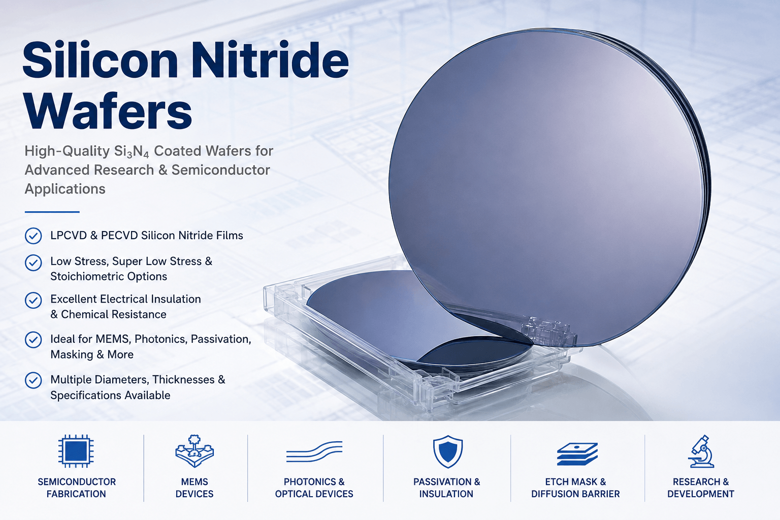
Silicon nitride (Si3N4) wafers are among the most widely used substrates in semiconductor manufacturing because of their outstanding electrical insulation, mechanical strength, chemical stability, and resistance to oxidation. Whether deposited by LPCVD or PECVD, silicon nitride films serve as reliable dielectric layers, diffusion barriers, passivation coatings, and etch masks for advanced device fabrication.
UniversityWafer offers silicon wafers coated with stoichiometric, low-stress, and super-low-stress silicon nitride films in a variety of diameters, crystal orientations, thicknesses, and resistivities. Our substrates are trusted by research laboratories, universities, government agencies, and commercial semiconductor manufacturers around the world.
Common Applications
- MEMS fabrication and microelectromechanical devices
- Photonic integrated circuits (PICs)
- Optical waveguides and resonators
- Semiconductor process development
- Surface passivation layers
- Diffusion and oxidation masking
- Microfluidic devices
- Sensors and biosensors
- Power electronics research
- Thin-film deposition studies
Available Options
Our silicon nitride substrates can be supplied with LPCVD or PECVD silicon nitride, custom film thicknesses, polished or double-side polished silicon, various crystal orientations including <100> and <111>, and prime or test grade wafers to meet both research and production requirements.
Get Your Silicon Nitride Wafer Quote FAST!
Need a custom silicon nitride wafer for your research or production process? Our engineers can help you select the ideal substrate, film thickness, stress level, and wafer specifications for your application.
Get Your Silicon Nitride Wafer Quote FAST! Or Buy Online and Start Researching Today!
What Are Silicon Nitride Wafers?
A silicon nitride wafer consists of a silicon substrate coated with a thin film of silicon nitride (Si3N4), one of the most important dielectric materials used in modern semiconductor manufacturing. Silicon nitride films provide exceptional electrical insulation, excellent mechanical strength, low defect density, and high resistance to moisture, chemicals, and thermal oxidation. These properties make silicon nitride an ideal material for integrated circuits, MEMS, photonics, sensors, and advanced research applications.
Silicon nitride coatings are commonly deposited using Low Pressure Chemical Vapor Deposition (LPCVD) or Plasma Enhanced Chemical Vapor Deposition (PECVD). LPCVD produces dense, high-quality films with excellent uniformity and chemical resistance, while PECVD enables lower-temperature deposition, making it suitable for temperature-sensitive processes and multilayer device fabrication.
Key Properties of Silicon Nitride
- Excellent electrical insulation and dielectric performance
- High hardness and mechanical durability
- Superior chemical and corrosion resistance
- Excellent oxidation resistance at elevated temperatures
- Low moisture permeability for device protection
- Effective diffusion barrier against dopants and contaminants
- Compatible with standard CMOS and MEMS fabrication processes
Research & Industrial Applications
Researchers and semiconductor manufacturers use silicon nitride wafers for a broad range of applications, including dielectric layers, passivation coatings, photonic integrated circuits, optical waveguides, biosensors, MEMS devices, microfluidics, high-frequency electronics, and thin-film process development. Their excellent optical transparency across visible and near-infrared wavelengths also makes silicon nitride a preferred platform for integrated photonics and quantum technologies.
Choosing the Right Silicon Nitride Wafer
Selecting the appropriate silicon nitride wafer depends on several factors, including deposition method, film thickness, residual stress, wafer diameter, crystal orientation, resistivity, surface finish, and intended device application. UniversityWafer supplies both standard and custom silicon nitride coated wafers with specifications tailored for semiconductor fabrication, academic research, photonics, MEMS, and prototype development.