
We are fabricating silicon photonic waveguides for operation at 1.55 μm and are looking for high-quality SOI wafers with a 220 nm device layer and 2 µm buried oxide. We would also like pricing for silicon nitride and lithium niobate substrates for integrated photonic device research.
Get Your Photonics Wafer Quote FAST!
UniversityWafer supplies high-quality photonics wafers and optical substrates for universities, research institutes, government laboratories, and commercial manufacturers. Whether you are developing silicon photonics, photonic integrated circuits (PICs), waveguides, lasers, optical sensors, or quantum devices, we can provide the substrate that best fits your application.
A university photonics researcher recently requested:
Photonics Substrates Available
- Silicon-on-Insulator (SOI) for silicon photonics
- Silicon wafers for optical device fabrication
- Silicon nitride substrates
- Gallium arsenide (GaAs)
- Lithium niobate (LiNbO3)
- GaN on sapphire
- Custom diameters, orientations, thicknesses, and surface finishes
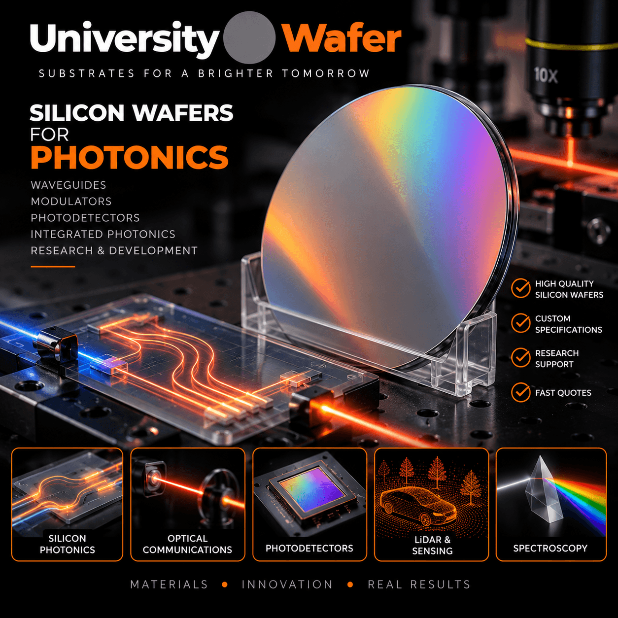
Our engineering team can help you select the ideal wafer for photonic integrated circuits, optical waveguides, lasers, modulators, photodetectors, quantum photonics, LIDAR, fiber optic communications, and biomedical imaging systems.
Get Your Photonics Wafer Quote FAST! Or, Buy Online and Start Researching Today!
What Are Photonics Wafers?
Photonics wafers are high-performance semiconductor and optical substrates used to fabricate devices that generate, guide, detect, and manipulate light. Unlike conventional electronic circuits that rely solely on electrons, photonic devices transmit information using photons, enabling higher bandwidth, faster data transfer, and lower power consumption for next-generation communication and sensing technologies.
UniversityWafer supplies research-grade substrates for silicon photonics, photonic integrated circuits (PICs), optical waveguides, lasers, modulators, photodetectors, quantum photonics, and biomedical imaging applications.
Common Materials for Photonics
Selecting the appropriate substrate depends on operating wavelength, optical transparency, refractive index, thermal conductivity, and device architecture.
| Material | Advantages | Typical Applications |
|---|---|---|
| Silicon | CMOS compatible, low optical loss at telecom wavelengths. | Silicon photonics, PICs, optical interconnects. |
| SOI | Excellent optical confinement and waveguide performance. | Integrated waveguides, modulators, resonators. |
| Silicon Nitride | Ultra-low optical loss over a broad wavelength range. | Frequency combs, biosensors, nonlinear photonics. |
| GaAs | Direct bandgap with efficient light emission. | Laser diodes, LEDs, photonic devices. |
| InP | High-speed optoelectronic performance at telecom wavelengths. | Optical communications, photonic integrated circuits. |
| Lithium Niobate | Exceptional electro-optic properties. | Optical modulators, quantum photonics. |
Photonics Applications
Photonic devices continue to replace traditional electronic systems in applications requiring higher bandwidth, improved sensitivity, and lower power consumption. Common research areas include:
- Photonic integrated circuits (PICs)
- Silicon photonics
- Optical communication systems
- Fiber optic transceivers
- Waveguides and optical resonators
- Laser diodes and VCSELs
- Optical sensors
- Quantum photonics
- Biomedical imaging
- LIDAR systems
- Machine vision
- Optical computing
Why Researchers Choose UniversityWafer
UniversityWafer supplies a broad portfolio of semiconductor and optical substrates for universities, government laboratories, startups, and commercial manufacturers. Standard and custom wafer diameters, orientations, doping levels, oxide thicknesses, epitaxial structures, and surface finishes are available to support advanced photonics research and production.
Our engineering team can recommend the ideal substrate for silicon photonics, integrated optics, laser fabrication, photodetectors, nonlinear optics, and quantum device development.
Complementary Materials
In addition to photonics wafers, UniversityWafer offers germanium, GaN on sapphire, graphene, sapphire, single crystal quartz, and numerous specialty materials for optoelectronics, quantum technologies, MEMS, and semiconductor fabrication.