Sapphire Wafers for Optical Device Fabrication
A PhD optical engineering candidate requested the following quote:
Are you providing 2" single crystal
sapphire substrates for optical devices (Epitaxy-ready sapphire
substrates)? Could you please give me a quotation? Following are some
parameters that I concern most for 50.8mm c-plane sapphire substrates:
- c-plane sapphire substrates, miscut by?
- Thickness 430 um?
- Single-sided polished or double-sided polished?
- Please provide quotation for quantities of 50, 1,000 and 10,000
respectively.
Reference #2468274 for specs and pricing.
Get Your Quote FAST! Or, Buy Online and Start Researching Today!
Indium Gallium Arsenide (InGaAs) Substrates to Fabricate Optical Devices
A Senior Engineer,Optical Devices requested the following quote:
I know you generally sell bulk semiconductor substrates, but do you guys get wafers that include working epi designs? Specifically, I'm looking for residual GaAs or InP/InGaAs growths for optical devices such as VCSELs (full or partial growth) or photodiodes. I'm sure that such wafers are not readily available for IP reasons, but maybe some simple design or dis-qualified wafer growths might be available?
Reference #131359 for specs and pricing.
Bonding Silicon Wafer with UV-Curable Epoxy for Optical
Devices
A company manufacturing communications devices requested the following quote:
We are looking for a few pyrex wafers, preferably with 200 mm diameter,
but 150 mm diameter is acceptable. Maximum thickness 1 mm, but thinner
ones (500 um or 750 um) are strongly preferred. The wafers require a good
flatness for bonding to 8-inch silicon wafer through epoxy. Only a single
side polish is required.
We are bonding it to a silicon wafer with UV-curable epoxy for optical devices.
Please let us know your availability of such wafers. If so, a quote will
be appreciated!
Reference #162167 for specs and quantity.
SOI Wafers To Fabricate Optical Devices
A Nanotechnology Researcher Requested the Following Quote:
Do you have any information on the original source of these wafers, or data sheets, what the top surface is like, and the consistency of the thickness. I want them for optical devices so these are important parameters.
Please quote me for 1, 2 ,5 and 10 of the wafers below:
SOI Item 1774
100mm P/B (100) 10-20 ohm-cm DSP 500um
Device 340nm
Oxide 1um
Reference #169573 for specs and pricing.
Gallium Nitride (GaN) Substrates for Optical Device Fabrication
A PhD student requested the following quote:
Here are the specs of the wafers. I'm not quite sure about some of them. We will be working on optical devices which require minimum absorption, thus the GaN has to be undoped? The silicon substrate can be either p or n doped since we will undercut the silicon and release the GaN layer in the end. Also would a thin buffer layer of AlN between GaN and Si improve the quality of the GaN? Thanks.
Diameter: Preferably to be 4 inches
Doping: Not sure
Orientation: Not sure
Resistivity: Not sure
Thickness: 120 nm GaN on 500 um Si
Quantity: 5pcs
Reference #221211 for specs and pricing.
Fused Silica Substrates to Fabricate Optical Devices
A research associate requested the following quote:
I am looking for 4-inch or 2-inch fused silica wafers for optical devices. The wafer need to be transparent for visible lights and should be able to deposit metal on one side. I noticed that you have several choices for these wafers. Do you have any recommendations which one would be most suitable for my case?
Reference # for specs and pricing.
Silicon Nitride to Fabricate Optical Devices
A graduate studdent studying at an ECE department requested the following quote:
I want to order wafers consisting of one stoichiometer LPCVD Si3N4 layer
isolated by Silica from Silicon substrate. The thickness of Si3N4 and
Silica layers may be around 300nm and 3 micrometers, respectively. Could
you send me some information about *price*(vs. the thickness of
materials), *lead time* and *minimum quality of wafers" we should order
for the following services:
- We send you our thermal oxidized silicon wafers, and only Si3N4 is
deposited on them;
- You do both the thermal oxidization and Si3N4 deposition on silicon
wafers.
Which one do you recommend or prefer?
We want to fabricate optical devices and do not care about the doping
and resistivity, and other electric properties of materials too much.
Other information about the silicon wafers are
Polish: single-side
Orientation: 100
diameter: 3 inches is preferable but 2-4 inches are also acceptable.
Therefore, Could you send me some information about the optical
characteristics of SiN layers, price (vs. the thickness of materials),
lead time and minimum quantity of wafers we should order? The thickness
of Si3N4 and Silica layers are around 200nm and 3000nm, respectively,
and we may alter the real thickness according to the price.
Besides, could you sell thermal oxidized silicon wafers?
Reference #105508 for specs and pricing.
Thick Thermal Oxide on Silicon to Fabricate Optical Devices
An Electrical Engineering Graduate Student requested the following quote:
I am Interested in have you grow a 6um thermal oxide on this wafer and then depositing a 250nm stiochiometric Si3N4 film on top of that. please send me a price quote for both the basic Si wafer and for the wafer with the above processing steps.
I will be making optical devices using the top nitride layer as a wave guide and the lower oxide as a cladding layer. Therefore I need the optical absorption in the nitride film to be as low as possible. Are your nitride films of optical quality?
Reference #109912 for specs and pricing.
What are Optical Devices?
Optical devices are instruments and tools that manipulate light to achieve specific results. These devices can range from simple lenses and mirrors to complex systems like microscopes, telescopes, and cameras. Here's a brief overview of some common optical devices:
-
Lenses: Lenses are transparent objects, typically made of glass or plastic, with at least one curved surface. They focus or disperse light rays to form images. Lenses are found in a wide range of applications, from eyeglasses to camera systems.
-
Mirrors: Mirrors reflect light, allowing them to create images or direct light beams. They come in various shapes, such as flat (plane mirrors), concave, and convex, each with distinct imaging properties.
-
Telescopes: These devices use a combination of lenses and/or mirrors to observe distant objects. Telescopes can be optical, designed for visible light, or specialized for other types of electromagnetic radiation (e.g., radio telescopes).
-
Microscopes: Microscopes magnify small objects or details that are too tiny to be seen with the naked eye. They usually consist of a combination of lenses to achieve high magnification and fine detail resolution.
-
Cameras: Cameras capture images of scenes or objects. They typically include a lens system for focusing, a mechanism to control the amount of light entering (aperture), and a sensor or film to record the image.
-
Prisms: Prisms are optical elements with flat, polished surfaces that refract light. They are often used to break light into its constituent spectral colors and for reflecting light at specific angles.
-
Fiber Optics: These involve the transmission of light through thin, flexible fibers, usually made of glass or plastic. Fiber optics are crucial in telecommunications, medical imaging, and endoscopy.
-
Spectacles and Contact Lenses: These are corrective optical devices designed to compensate for vision imperfections like nearsightedness, farsightedness, and astigmatism.
-
Laser Devices: Lasers emit highly focused, coherent, and monochromatic beams of light. They are used in a wide array of applications, including surgery, data storage, cutting and welding materials, and in scientific research.
Each of these devices leverages the principles of optics, the branch of physics concerned with the behavior and properties of light, including its interactions with matter. The design and use of optical devices are fundamental in numerous scientific, industrial, and consumer applications.
What Substrates are Often Used to Fabricate Optical Devices?
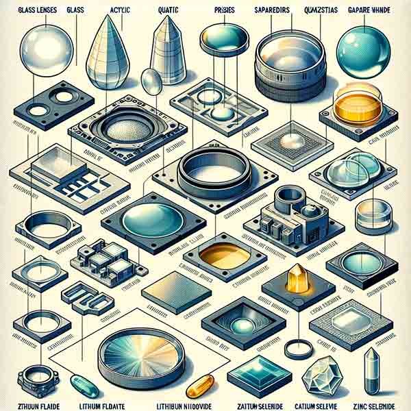
Optical devices are typically fabricated using a variety of substrates, depending on the application and the specific requirements of the device. These substrates are chosen for their optical properties, such as transparency, refractive index, and resistance to environmental factors. Some of the most commonly used substrates include:

-
Glass: This is the most traditional and widely used substrate for optical devices. Different types of glass, such as borosilicate, soda-lime, and fused silica, offer varying degrees of optical clarity, thermal stability, and resistance to chemical corrosion. Glass is used in lenses, prisms, mirrors, and windows.
-
Plastics or Polymers: These materials are increasingly popular due to their versatility, light weight, and lower cost compared to glass. Polymers such as acrylic (PMMA), polycarbonate, and polyethylene terephthalate (PET) are commonly used in lenses, especially for eyewear, and in other optical components like light guides and diffusers.
-
Silicon: Silicon is primarily used in the fabrication of optical components for infrared applications. It's also the basis for most semiconductor devices, which are crucial in optoelectronics.
-
Quartz and Fused Silica: These materials are used for high-precision and high-temperature applications. They are ideal for ultraviolet and infrared optics due to their high transmission and low thermal expansion properties.
-
Sapphire: Known for its hardness and durability, sapphire is used in demanding environments, such as in aerospace and military applications. It's also used for high-performance windows and lenses.
-
Germanium: This is another material used primarily for infrared optics. Germanium lenses and windows are common in thermal imaging and night vision technology.
-
Fluorides (e.g., Calcium Fluoride, Magnesium Fluoride): These materials are used in ultraviolet and infrared applications, including in lenses and windows for lasers and astronomical telescopes.
-
Zinc Selenide (ZnSe): This is a popular choice for infrared applications, especially in CO2 laser systems, due to its low absorption of infrared light.
-
Crystal Substrates (e.g., Lithium Niobate, Gallium Arsenide): These are used in specialized applications, including nonlinear optics and electro-optic modulators.
Each substrate offers unique advantages and challenges, and the choice of material is crucial in determining the performance and suitability of the optical device for its intended application. Advances in material science continue to introduce new substrates and improve the capabilities of existing ones in the realm of optics.
What Silicon Doping Works Best for Optical Device Fabrication?
A graduate student asked the following:
Question:
Do you know if they are appropriate for optical devices in terms of doping? RFQ#220012.
Answer:
Silicon doping in optical device fabrication is a nuanced topic, as the choice of dopant depends on the specific application and the desired properties of the silicon. In the context of optoelectronics and photonics, where silicon is used not just as an electronic material but also for its optical properties, the choice of doping can significantly impact the performance of the device. Here are some common dopants and their typical applications:
-
Phosphorus (P): Phosphorus is a common n-type dopant in silicon. It's used to increase electron concentration, thereby enhancing electrical conductivity. Phosphorus-doped silicon is often used in photodetectors, solar cells, and some types of light-emitting diodes (LEDs).
-
Boron (B): Boron is the most common p-type dopant for silicon. It's used to increase the hole concentration in the material. Boron-doped silicon finds application in p-n junctions in solar cells, photodiodes, and other semiconductor devices.
-
Arsenic (As) and Antimony (Sb): These are also used as n-type dopants, similar to phosphorus, but they offer different diffusion characteristics and electrical properties. They can be used in specific applications where these particular properties are desired.
-
Indium (In) and Gallium (Ga): These p-type dopants are less common but can be used for certain specialized optical applications, such as in the fabrication of photodetectors and infrared detectors.
The doping level also plays a critical role. Light doping is typically used in optical applications to maintain the semiconductor's transparency to light, while heavy doping can increase absorption or modify the refractive index of silicon, which can be advantageous in some photonic devices.
In silicon photonics, where silicon is used to guide and manipulate light, the goal is often to alter the material's refractive index slightly without introducing too much optical absorption. This is typically achieved with light to moderate doping levels.
In summary, the best silicon doping for optical device fabrication depends on the specific optical and electronic properties required for the device. Advances in silicon photonics and related fields continue to explore and optimize the use of various dopants for different optical applications.

