
I would like to get the quote for the below mentioned product with exact details. We need Lithium-Niobat wafers for the our QCLAM spectrometer. They should be like: 1 inch Z-cut optical grade LN, no flat, 0.2mm thickness, DSP We need approximately 10 pieces.
Optical Grade LiNbO3 for Use With QCLAM Spectrometer
A nuclear physics engineer requested a quote for the following:
Reference #272391 for specs and pricing.
Lithium Niobate Substrate Research Applications
Below are just a few of the applications researchers use LiNbO3 wafer applications. Click the links to learn more.
- Optical Waveguides
- Biosensors
- Surface Acoustic Wave Generation (SAW)
- Smartphones RF filters
- Quantum Acoustics
- Customized to meet your needs
Get Your LiNbO3 Wafer Quote FAST! Or, Buy Online and Start Researching today!
LiNbO3 Wafers for SAW Applications
A physics Ph.D. Candidate requested a quote for the following:
I am looking for 3 wafers of 128°-X Lithium Niobate wafers for SAW applications fr Surface Acoustic Wave Generation (SAW).
So I think single sided polished as flat as possible and the thickness of the waver shouldn't be too thick so I can cut it to smaller pieces.
Reference #226902 for specs and pricing.
Lithium Niobate Wafers for Optical Waveguide Fabrication
A professor of electrical engineering requested the following quote:
I am trying to get some Pockels switches going and need LiNbO (lithium niobate) substrates for optical waveguides. I am also trying to get a spontaneous parametric down conversion to get superposed photons by coincidence detection using BBO crystals. If you can help in any of that it would be appreciated!
Reference #218828 for specs and pricing.
LiNbO3 Substrates for Biosensor Fabrication
A PhD candidate requested the following quote:
We are participating in a competition and we will need some Lithium Niobate wafers to fabricate our final devices.
(Specifically we need five (5) 64 Y-X cut Lithium Niobate wafers)
We need 5 wafers of the following specs:
- Diameter: 3 inch (7.62cm)
- Cut: 64 Y - Cut (X propagation)
- Thickness: 0.5mm
- Reference Flat: doesn’t matter
- And, single side polished.
Reference #226188 for specs and pricing.
What LiNbO3 Substrates Used to Fabricate Smartphones RF Filters?
A corporate MEMS researcher requested the following quote:
Do you know of any high volume sources for 6” Lithium Tantalate or Niobate wafers? We have a high volume application that requires this material, but we cannot process 4” wafers.
Well this is for smartphones RF filters, so the volumes will be extremely high, but we first need to prove the product with prototypes and qualification volumes (100s of wafers)
We’re fairly flexible on specs.. since there are several different designs we can pursue. We prefer notched wafers – and are willing to by full boules if needed. Can you get anything on 150mm?
I also have learned that what we actually want is. 1um thin film of LN or LT on 6” Silicon. Any chance you know of a way to source such wafers?
Reference # for specs and pricing.
Lithium Niobate (LiNbO3) Wafer Carrier
Increasing demand for optical-fiber-based communication systems will increase the demand for LiNbO3 modulators.
LiNbO3 applications include:
- Q-switching devices
- High-performance gyroscope
- Accelerators and accelerometer sensors
- MEMS devices
Lithium Niobate is an optical material. LiNbO3 substrates are widely used in the following Device applications:
- Surfaced acoustic devices
- Integrated optic devices
- Wavelength generation
Lithium Niobate LiNbO3 substrates are often used in the following:
- Electro-Optic
- Ferroelectric
- Domain Engineering
- Beam Deflectors and Switches
- Optical Waveguides
- Intensity Modulators
- Phase Modulation
- Polarization Control
- Quasi-Phase Matching
- Photonic Crystals
- Analog Fiber Optic Links
- Electric Field Sensing
- Photonic Signal Processing
- Digital Data Transmission
- Optical Frequency Conversion.
Researcher Use of Lithium Niobate (LiNbO3) Wafers
Researchers use LiNbO3 windows for modeling, design, and characterization of lithium niobate devices for sensing, modulation, and optical frequency conversion.
SAW Grade Lithium Niobate Wafers
UniversityWafer, Inc. and partners have to ability to grow LiNbO3 crystrals, as well as provide wafer lapping, polishing and quality control.
Material |
LiNbO3 wafers (White or Black) |
|
| Curie Temp | 1142±2.0℃ | |
| Cutting Angle | X/Y/Z/Y36/Y41/Y64/Y128/etc | |
| Diameter/size | 3”/4”/6"LN wafer & 8"under R/D | |
| Tol(±) | <0.20 mm | |
| Thickness | 0.18 ~ 0.5mm or more | |
| Primary Flat | 22mm /32mm /42.5mm /57.5mm | |
| LTV (5mmx5mm) | <1µm | |
| TTV | <3µm | |
| Bow | -30<bow<30 | |
| Warp | <40µm | |
| PLTV(<0.5um) | ≥95%(5mm*5mm) | |
| Ori Flat | All available | |
| Surface Type | Single Side Polished /Double Sides Polished | |
| Polished side Ra | <0.5nm | |
| Back Side Criteria | General is 0.2-0.5µm or as customized | |
| Edge Criteria | R=0.2mm or Bullnose | |
| Wafer Surface Criteria | Transmissivity | general:5.9x10⁻¹¹<s<2.0*10-10 at 25℃ |
| Contamination, | None | |
| Particles ¢>0.3 µ m | <= 30 | |
| Scratch , Chipping | None | |
| Defect | No edge cracks, scratches, saw marks, stains | |
Optical Grade Lithium Niobate Wafers
Below are specifications for our optical grade LiNbO3 wafers.
Material |
Optical Grade LiNbO3 wafes (White or Black) |
|
| Curie Temp | 1142±2.0℃ | |
| Cutting Angle | X/Y/Z etc | |
| Diameter/size | 2”/3”/4” | |
| Tol(±) | <0.20 mm | |
| Thickness | 0.18 ~ 0.5mm or more | |
| Primary Flat | 16mm/22mm /32mm | |
| TTV | <3µm | |
| Bow | -30<bow<30 | |
| Warp | <40µm | |
| Ori Flat | All available | |
| Surface Type | Single Side Polished /Double Sides Polished | |
| Polished side Ra | <0.5nm | |
| S/D | 20/10 | |
| Edge Criteria | R=0.2mm or Bullnose | |
| Optical doped | Fe/Zn/MgO etc for optical grade LN< wafers | |
| Wafer Surface Criteria | Refractive index | No=2.2878/Ne=2.2033 @632nm wavelength |
| Contamination, | None | |
| Particles ¢>0.3 µ m | <= 30 | |
| Scratch , Chipping | None | |
| Defect | No edge cracks, scratches, saw marks, stains | |
Lithium Niobate Photovoltaic Applications
LiNbO3 product development is underway to develop a silicon wafer that can be sawn with a galvanic blade to produce high-performance photovoltaic and optoelectronic clamps and other applications.
Lithium Niobate Wafers To Convert Heat to Electrical Energy
Researchers have used the following wafers for their research:
| Dia | Ori | Thickness | Surface Finish | Brand /Grade | Top side Ra | Backside Ra |
| 76.2+/-0.3mm | Z-Cut | 0.15mm+/-0.03 | DSL | SAW | GC#1000 | GC#1000 |
What LiNbO3 Substates Should I use to Convert Heat to Electrical Energy
Researchers have used the following LiNbO3 wafers for their research converting heat into electricity.
Item# |
DiA |
Ori |
Thick |
POL |
Material |
Brand /Grade |
Top side Ra |
Backside Ra |
| 256724 | 76.2+/-0.3mm | Z-Cut | 0.15mm+/-0.03 | DSL | LiNbO3 | SAW | GC#1000 | GC#1000 |
What Are The Different Cuts, (X,Y,Z, etc.) and what the differences is between SSP and DSP?
- first, the price of one piece of "LiNbO3 SAW grade, Y-cut, 10x10x0.5mm, SSP " is $Contact Us
- Taking LN wafer as an example, the Y plane is the polar plane and hydrofluoric acid is used for wet etching.
The corrosion rate of front and back of the wafer is different.The Angle (0°, 90°, 90°) means that the -Y side
of the wafer is the polished surface, and there is a reference edge on the +Z end of the wafer.The Angle (180°, 90°, 90°)
indicates that the +Y side of the wafer is the polished surface and that the reference edge is still on the +Z end of the wafer.
please refer to the following picture shows:
Rotate the coordinate system (X, Y, Z) to the Euler Angle diagram of (χ1, χ2, χ3)

SAW wafer coordinate system

Also, DSP means double sides polished, and SSP means single side polished and the other side usually lapped with Ra around 0.2-0.5um.
Lithium Niobate FAQs
Typical questions and answers:
Question:
Could you also let me know if you supply full X-cut LiNbO3 wafers? On the website I only see Y-cut.
Answer:
No! It is not available besides by bonding process. Bonding a thick LN layer (>5um) on Silicon can not produce nano grade thin film.
Question:
Can I also ask if Depositing LN directly on HR-Si is possible?
Answer:
Yes! X-cut LNOI Wafer
4inch X-Cut LN thin film:300nm/ SiO2:2μm (thermal) / Silicon substrate: 0.5mm (high resi.>10000Ω-cm)
Reference #264464 for specs and pricing.
X-LN thin film to Research Light-Matter Interaction in Condensed Matter Physics
A senior scientist professor requested the following quote:I am interested in the following LNOI wafers. Can you send me a quote? -Feng X-LN thin film:300nm/ SiO2:2μm (thermal) / Silicon substrate: 0.5mm (high resi.>10000Ω-cm) X-LN thin film: 400nm/ SiO2:2μm (thermal) / Silicon substrate: 0.5mm (high resi.>10000Ω-cm) X-LN thin film: 500nm/ SiO2:2μm (thermal) / Silicon substrate: 0.5mm (high resi.>10000Ω-cm).
I am inquiring for two different types of wafers.
- SOI wafer with 200nm or 340nm silicon device layer and a BOX layer of 1-3 micron thickness.
- X-LN thin film on SiO2/Si. For example, this one listed on your website.
- X-LN thin film: 300nm/ SiO2:2μm (thermal) / Silicon substrate: 0.5mm (high resi.>10000Ω-cm).
We have those required LNOI wafer from in stock,Spec. fully matched,Pls see below for the offer:
- X-LN thin film:300nm/ SiO2:2μm (thermal) / Silicon substrate: 0.5mm (high resi.>10000Ω-cm)
- X-LN thin film: 400nm/ SiO2:2μm (thermal) / Silicon substrate: 0.5mm (high resi.>10000Ω-cm)
- X-LN thin film: 500nm/ SiO2:2μm (thermal) / Silicon substrate: 0.5mm (high resi.>10000Ω-cm)
Reference # 257622 for specs and pricing.
Lithium Niobate Rods
A postdoctoral researcher requested a quote for the following:
We previously brought LiNbO3 Rod Diam 20mm, 70mm long, Y-36 Degree cut Double ends Au Coated. We were wondering if different lengths are available. Are there rods with lengths between 35 mm and 60 mm available? The diameter needs be smaller than the length. We still need the Y-36 Degree cut Double ends Au Coated. Please let me know if such rods are available, quote for 3 rods and lead time.
Please reference 271452 for specs and pricing.
Lithium Niobate Substrates Used in QCLAM spectrometer
A Phd candidate requested help finding the correct LiNbO3 wafer for their research:
Reference #272391 for specs and pricing.
How to Exploit Maximum Electro-Optic Effect of LiNbO3?
A CTO of a start up requested the following device fabrication quote:
Id like to receive a quotation for the following:
- Nr. 10 substrates LiNbO3 optical grade, Z-cut, 10x10x0.1mm, DSP
- Nr. 10 substrates LiNbO3 optical grade, Z-cut, 10x10x0.5mm, DSP
Is it possible to have HR dielectric coating on both sides of LiNbO3 substrate?
I am still making up my mind on which cut order to exploit maximum electro-optic effect of LiNbO3 in my configuration (applied field parallel to optical propagation direction).
I will order substrate without coating as I want to implement my own coating process in clean room. However, which reflectivity can you reach with HR coating on 0.5 mm substrates? In your opinion, is it possible to build a process in order to perform a double side HR coating?
UniversityWafer, lnc. Quoted:
We are not sure whether we can get 0.1mm thick successing, if you willing, we will try it for you, but we can not do HR dielectric coating for 0.1mm.
See our quotation below:
- LiNbO3 optical grade, Z-cut, 10x10x0.1mm, DSP
- LiNbO3 optical grade, Z-cut, 10x10x0.5mm, DSP
Reference #247859 for specs and pricing
LiNbO3 Substrates for Surface Acoustic Wave Experiment
A scientist requested a quote for the following:
I am looking for LiNbO3 substrates for surface acoustic wave experiment with thin magnetic films. I would like to ask a rough quotation and delivery time. Also, what are the differences between X, Y, and Z cut (with different angles)?
I would like to have 20 pieces of 10X10 mm; 0.5 mm thick; one-side polished; Y; 128deg cut LiNbO3 substrates.
UniversityWafer, Inc. Quoted:
We'll issue you a best offer as soon as get your q;ty and spec requirement in detail. Meanwhile, the two typical drawings for your refer and hope to help you better understand it X and Y-cut.

Reference #271679 for specs and pricing
Z-Cut Lithium Niobate for Pyroelectric Infrared Detectors
A corporate scientist requested the following:
I have a question. This is a pyroelectric infrared detector. Do I need optical grade? Can you quote me the following.. Lithium Niobate Z-Cut 27mm diameter +/- .5mm .5 mm thick Polish both side 10/5 scratch/dig Overcoat both surfaces 100 Angstroms of chromium. (no gold) Please quote SAW grade and Optical grade.
Reference #274452 for specs and pricing.
What is a Quartz Resonator?
Often referred to as “Xtal” in circuit diagrams these electronic components work on the principle of converting the mechanical resonance of a vibrating crystal of piezoelectric material into an electrical signal with a fixed frequency. They are widely used for a number of applications from simple clock oscillators, to sophisticated filters.
Quartz crystals exhibit a remarkable number of physical properties which make them particularly well suited to use in crystal resonator technology. Their material properties are extremely stable with temperature and other environmental conditions and highly repeatable from one crystal to the next. Their acoustic loss or internal friction is also very low. These characteristics combine to give quartz crystal resonators a Q factor which is orders of magnitude better than the best LC circuits.
When a dc voltage is applied across the faces of a quartz crystal it causes it to resonate at its natural operating frequency. This is typically at least a third of the fundamental mode frequency and can be as high as several MHz. A resonator may be designed to operate at a single operating frequency or at multiple frequencies at varying resonant modes referred to as overtones.
The resonator’s mode of operation depends on the crystal geometry and cut. For a frequency above 1 MHz most crystals are designed to operate in either the thickness shear or face shear modes. The choice of cut is important for a number of reasons including frequency stability, phase noise and cost.
Related Substrate and Photonics Resources
Why Use Lithium Nioabate Wafers?
It can be hard to keep up with the latest advances in materials technology, even if you're an engineer.
Problem: Materials technology is advancing faster than ever before and it's becoming harder and harder to keep up. It can be a challenge to know which materials are worth researching.
 Solution: Lithium niobate wafers are a great substrate for your research! LiNbO3 wafers have unique optical and piezoelectric properties that make them perfect for a wide range of applications. They're also stable under high-power conditions, making them ideal for SHG lasers and other optoelectronic devices.
Recently Lithium Niobate (LiNbO3) substrates are increasingly used to fabricate integrated optical devices. By reducing waveguide dimensions, LiNbO3 electro-optical modulators can create new design paradigms that enable a wide range of applications, such as drive voltage and the expansion of the spectrum of nonlinear optical applications for high-performance optics.
What are Lithium Niobate (LiNbO3) Wafers?
Lithium niobate is a crystal material that is often used to create wafers for use in photonic, piezoelectric, and electro-optic applications. These wafers are typically thin and flat, and are produced through processes such as crystal growth, slicing, and polishing. Lithium niobate wafers are known for their high refractive index, piezoelectric properties, and nonlinear optical response, making them useful for a wide range of applications, including telecommunications, sensing, and computing.
Researches have investigated the photorefractive centers of LiNbO3 and related systems. Jermann, F., and Kratzig, E. studied light-induced charge transport in pure LiNbO3, and Kurz, H., and Wohlecke, M., and Broderick, D. C., M., and S. L. studied hexagonally-poled LiNbO3 for laser diodes. Rams, B., and S. Klauer have investigated the protonic conductivity of LiNbO3.
The ring modulator made of LiN is the first of its kind to demonstrate a large third-order intermodulation distortion spurious free dynamic range at 10 GHz and 1 GHz. The ring modulator's linearity is an order of magnitude higher than that of silicon ring modulators based on the plasma dispersion effect. Further, this material has a second-order susceptibility, making it an attractive material for use in compact modulators for analog optical links.
What is Lithium Niobate Refractive Index?
Lithium niobate is a crystal that has a refractive index of around 2.2. This means that light traveling through the crystal will be bent by an angle that is determined by the refractive index of the material. The refractive index of a material is a measure of how much the speed of light is reduced when it passes through the material. In general, materials with a higher refractive index will bend light more than materials with a lower refractive index.
What is Integrated Photonics on Thin-Film Lithium Niobate Wafers?
Integrated photonics involves the integration of multiple photonic components onto a single platform, such as a thin film of lithium niobate. This technology allows for the creation of compact, efficient, and high-performance photonic devices that can be used in a wide range of applications, including telecommunications, sensing, and computing.
Does Lithium Niobate Have Piezoelectric Characteristics?
Lithium niobate is a piezoelectric material, which means that it exhibits the piezoelectric effect. This effect is the ability of certain materials to convert mechanical stresses or strains into electrical charges, and vice versa. When a mechanical force is applied to lithium niobate, it produces a voltage, and when a voltage is applied, it produces a mechanical strain. These piezoelectric properties make lithium niobate useful in a variety of applications, including pressure sensors, transducers, and actuators.
LiNbO3 is an excellent material for optoelectronic devices. It has unique piezoelectric and optical properties. Its mechanical stability makes it a desirable candidate for high-power SHG lasers. It is an excellent semiconductor for optical modulators and enables tunable IR outputs. It also exhibits outstanding spectral sensitivity. The next-generation materials are now being researched for their use in a wide range of applications.
In addition to its optical properties, LiNbO3 is also used for high-density storage. The material is a great candidate for high-density optical elements. Its low density makes it an excellent material for lasers. Further, it can be incorporated into various types of electronic components. In addition, it can be used as a photonic crystal. The main advantage of LiNbO3 is that it has a high refractive index.
Because of its strong piezoelectric properties, LiN is an ideal candidate for making ultra-high-power ultrasonic transducers for Enhanced Oil Recovery. This paper is intended to provide the basis for future research on this oil production technique. The high-power transducer was used to reduce the viscosity of super heavy oil. This study also demonstrates the effectiveness of LiN in reducing viscosity.
Because of its nonlinear optical properties, LiNbO3 is a good candidate for the second harmonic generator in a Nd:YAG laser. Because of its high photorefractive properties, it is a good candidate for semiconductor lasers. Further, it has excellent electrical properties, which make it a good choice for a second harmonic generator. However, the low optical performance of LiNbO3 may limit its use in certain applications.
The crystal is transparent and relatively hard, making it a good candidate for electro-optical applications. Its properties are useful in nonlinear lightwaves. For instance, it has a small refractory index, which makes it suitable for nonlinear communication. It can also be used for semiconductor devices, such as holographic storage. A large variety of uses are available in this material. It can be found in various sizes, including 2-2.5 inches.
The material is also useful for acoustic wave-filtering. It is a nonlinear material with high-frequency conductivity. Its nonlinear polarization properties make it a suitable material for ultrahigh-frequency acoustic applications. Its low-frequency characteristics make it a good candidate for use in radio frequency. For example, it can be used for radar. This material can also be used for the development of new technologies.
The multifunctional crystal lithium niobate has numerous applications in photonics, electronics, and optoelectronics. It has been widely used in semiconductor devices, and has a significant role in many emerging technologies. Integrated photonics is also becoming more widespread, and LiNbO3 has been found to be an excellent choice for this. Its ion-cut properties and low power consumption make it a valuable material for high-power, ultra-fast applications.
The chemical structure of lithium niobate is similar to that of lithium iodide. In a single crystal, the two ions are filled in order of "Li-Nb-vacancy-Li". Its electrochemical properties are a result of the asymmetric charge centers in the atoms. Thus, the energy in the electrochemically-reactive properties of Lithium niobate are correlated.
LiNbO3 Wafers for Acoustic Wave Research
Researcher Asks:
"We currently use the wafers to deposit metallic monolayers to lateron induce acoustic waves harsening the piezoelectric properties of the LiNbO3.
After testing some LiNbO3 wafers we recently purchased, we decided that they worked well for our purposes. I would then like to ask you for a new formal quote because we are willing to get more of the same product.
The specifications of the wafers are: LiNbO3 wafers, SAW grade, DSP, 76.2 mm diameter, 0.5 mm thick, 128Y Ori Last time we got 10 pieces. This time we are even planning to get more of them (20 or so). "
UniversityWafer, Inc. Quoted:
Price depends on quantity. Please contact us and reference #260387
| Surface | Outer Diameter | Ori | Thickness | Primary Flat | Material | Brand/Grade | Top side Ra | Backside Ra |
| DSP | 76.2+/-0.2mm | 128Y | 0.5+/-0.03mm | 22mm | LiNbO3 | SAW | <1nm | <1nm |
LiNbO3 Wafer to Optimize PLD Parameter
An postdoc from a European university used the following substrate for their research:
The LiNbO3 wafer will be used to optimize of PLD parameter of LiNbO3
thin films. The LiNbO3 thin films will be
applied in test structures for surface acoustic
wave (SAW) devices (e.g. for biosensors).
Results for SAW devices based on LiNbO3
thin films will be compared to our results for
SAW devices based on (K,Na)NbO3 thin films.
- It's about basic research on SAW devices.
- LiNbO3 wafer for homoepitaxial growth of LiNbO3 thin films
Please reference #271384 for specs and pricing.
Lithium Niobate (LiNbO3) Substrates
Many research clients use Lithium Niobate wafers for the following purposes:
- Telecom
- Mobile Phones
- Optical Modulators
- Surface Acoustic Wave Devices
LiNbO3 Wafer in stock
4 inch, 0.5mm thickness, Z-cut, optical grade, DSP
Other Inventory includes the following. Let us know if you need custom specs!
LiNbO3 SAW grade, 36 degree off Y-X cut with flat Ori: X cut or <11-20> , 20x20x0.5mm, SSP
LiNbO3 saw grade, X-cut, 10x10x0.5 mm, SSP
LiNbO3 saw grade, X-cut, 10x10x0.5 mm, DSP
LiNbO3 SAW grade, Y-cut, 10x10x0.5mm, SSP
LiNbO3 SAW grade, Y-cut, 36 degree off 10x10x0.1mm, DSP
LiNbO3 SAW grade, Y-cut, 36 degree off 10x10x0.5mm, SSP
LiNbO3 SAW grade, Z-cut, 10x10x0.5mm, SSP
LiNbO3 optical grade, Z-cut, 5x5x0.5 mm, SSP
LiNbO3 optical grade, X-cut, 10x10x0.1mm, DSP
LiNbO3 optical grade, X-cut, 10x10x0.5mm, DSP
LiNbO3 optical grade, X-cut, 10x10x1.0mm, DSP
LiNbO3 optical grade, Y-cut, 10x10x0.5mm , DSP
LiNbO3 optical grade, Z-cut, 10x10x0.1mm, DSP
LiNbO3 optical grade, Z-cut, 10x10x0.5mm, DSP
Mg doped LiNbO3 optical grade, Z-cut, 10x10x0.5 mm , DSP
Stoichiometric LiNbO3 (SLN) Wafer, Z-cut, 10x10 x 0.5 mm , SSP
Stoichiometric LiNbO3 (SLN) Wafer, Z-cut, 10x10 x 0.5 mm Doulbe Side Polished (DSP)
Fe doped LiNbO3 crystal, Z-cut, 10x10x0.5 mm , DSP
LiNbO3 Wafer, Optical Grade, X-cut, 3" x 0.5mm, DSP
LiNbO3 saw grade, X-cut, 2" wafer, SSP
LiNbO3 Saw Grade Wafer, X-cut, 3" x0.5 mm, Single Side Polished (SSP)
LiNbO3 saw grade wafer, Y-cut, 2" dia. x0.5 mm thick, SSP
LiNbO3 saw grade wafer, Y-cut, 3" dia. x 0.5 mm thick, SSP
LiNbO3 saw grade, Z-cut, 2"x0.5mm wafer, SSP
LiNbO3 saw grade wafer, 128 deg. Y/X cut, 3" x1.0 mm, DSP
LiNbO3 saw grade wafer, 128 deg. Y-X cut, 3" x0.5 mm, DSP
LiNbO3 saw grade wafer, 128 deg. Y-X cut, 4" dia x0.5 mm, DSP
LiNbO3 saw grade wafer, 128 deg. Y-X cut, 4" dia x1.0 mm, DSP
LiNbO3 saw grade wafer, Z-cut, 3" x0.5 mm , SSP
LiNbO3 saw grade wafer, 128 deg. Y/X cut, 3" x1.0 mm, DSP
LiNbO3 saw grade wafer, 128 deg. Y-X cut, 3" x0.5 mm, DSP
LiNbO3 saw grade wafer, 128 deg. Y/X cut, 3" x1.0 mm, DSP
LiNbO3 saw grade wafer, 128 deg. Y-X cut, 3" x0.5 mm, DSP
LiNbO3 saw grade wafer, 128 deg. Y-X cut, 4" dia x0.5 mm, DSP
LiNbO3 saw grade wafer, 128 deg. Y-X cut, 4" dia x1.0 mm, DSP
LiNbO3 saw grade wafer, 128 deg. Y-X cut, 4" dia x0.5 mm, DSP
LiNbO3 saw grade wafer, 128 deg. Y-X cut, 4" dia x1.0 mm, DSP
LiNbO3 wafer, optical grade, Y-cut, 3" x0.5mm, DSP
LiNbO3 saw grade wafer, 128-deg. Ycut with flat, 3" x0.5 mm, SSP
LiNbO3 saw grade wafer, 36-deg. Ycut without flat, 3" x0.5 mm, SSP
LiNbO3 saw grade wafer, 128 deg. Y-X cut, 4" dia x0.5 mm, SSP
LiNbO3 Wafer , optical grade, Z-cut, 3"x0.5mm, DSP
LiNbO3 saw grade wafer, 128 deg. Y/X cut, 3" x1.0 mm, DSP
LiNbO3 saw grade wafer, 128 deg. Y-X cut, 3" x0.5 mm, DSP
LiNbO3 saw grade wafer, 128 deg. Y-X cut, 4" dia x0.5 mm, DSP
LiNbO3 saw grade wafer, 128 deg. Y-X cut, 4" dia x1.0 mm, DSP
LiNbO3 saw grade wafer, 128 deg. Y/X cut, 3" x1.0 mm, DSP
LiNbO3 saw grade wafer, 128 deg. Y-X cut, 3" x0.5 mm, DSP
LiNbO3 saw grade wafer, 128 deg. Y-X cut, 4" dia x0.5 mm, DSP
LiNbO3 saw grade wafer, 128 deg. Y-X cut, 4" dia x1.0 mm, DSP
Lithium Niobate (LiNbO3) Definition
LiNbO3 is a crystal material with Curie temperature that falls within a specified value. LiNbO3 has a single domain structure that's created by a polarization process.
Large Diameter SAW Grade LiNbO3
150mm LiNbO3 128 Y-Cut 0.5um DSP Notch or 47.5+/02.5mm on +Z SAW Grade
Warp <40um
Bow <40um
TTV <10um
Roughness
-Top Side <1nm
-BackSide <1nm
Price depends on quantity.
Lithium Niobate on Insulator (LNOI)
UniversityWafer, Inc. and our partners can produce 300-900nm X-cut LN or Y42-cut LT thin film on SiO2 on silicon sub.
We also make some other customized thin film LN or LT wafers.
The price for one standard 4 inch LNOI wafer: Pleae contact us.
Now we have a few structures of favorable discounts (pls see below reference 60110992).
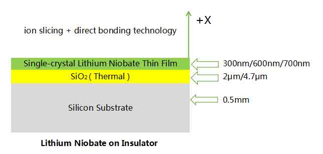
The pricing for many other structures all depends.
| X-LN thin film:300nm/ SiO2:2μm (thermal) / Silicon substrate: 0.5mm (high resi.>10000Ω-cm) |
$Contact Us |
| X-LN thin film:600nm/ SiO2:2μm (thermal) / Silicon substrate: 0.5mm (high resi.>10000Ω-cm) |
$Contact Us |
| X-LN thin film:600nm/ SiO2:4.7μm (thermal) / Silicon substrate: 0.5mm (high resi.>10000Ω-cm) |
$Contact Us |
| X-LN thin film: 400nm/ SiO2:2μm (thermal) / Silicon substrate: 0.5mm (high resi.>10000Ω-cm) |
$Contact Us |
| X-LN thin film: 500nm/ SiO2:2μm (thermal) / Silicon substrate: 0.5mm (high resi.>10000Ω-cm) |
$Contact Us |
What is Black Lithium Niobate (LiNbO3) Wafers and Its Benefits?
If you are wondering what Black Lithium Niobate is, you've come to the right place. Here you'll learn the science behind this material, how it's used, and why it's so useful for electronics applications. Here are some benefits of Black Lithium Niobate:
DC VAC measurements: DC voltages applied to the electrodes are converted to volts per ampere. The voltammetry used to measure the specific resistivity of Black Lithium Niobate reveals that the material has a high resistance compared to other materials. DC measurements are also used in many industries, and their high residivity makes them ideal for power applications. However, there is a caveat. Lithium Niobate is also a weak conductor. As a result, measurements should be conducted with a very high voltage.
The crystal structure of Black Lithium Niobate is complex. Because of its low temperature conductivity, it's often used in electronics as a battery. However, it has an advantage over conventional batteries in that it's more efficient and stable. However, the downside of Black Lithium Niobate is that it's prone to oxidation. So, it is better to use batteries with lithium-ion batteries than to rely on these.
A negative uniaxial crystal of Black Lithium Niobate (LiNbO3) displays a high degree of photorefractive property. It has been thoroughly characterized in optical measurements by Stanton, P.L., Graham, R.A., and Morris, R.W., and is useful for a wide variety of nonlinear applications. Its refractive properties make it ideal for various spectroscopic applications, including nonlinear optical polarization and photoelasticity.
The high degree of transparency and the low power consumption make Black Lithium Niobate an attractive material for many applications in electronics and photonics. Its outstanding electro-optic and electro-mechanical coupling properties have made it a useful material in various fields, from medical devices to consumer electronics. The chemical structure of LiNbO3 is similar to that of lithium iodide, and it has asymmetric charge centers.
The two most common materials used to make Black Lithium Niobate are Lithium Tantalate (LiAtO3) crystal substrate and rustless steel containers. Lithium columbate crystal substrate is a 400mm square piece of lithium in a rustless steel container. Generally, the amount of Zn in the mixture is less than 35% of the total mass ratio in a mixed system. There is also an organic silica gel in the mixture.
A recent study shows that floating electrode unidirec tional transducers have a directivity of 22 dB at 10 mK and 4.7 dB less insertion loss compared to standard interdigital transducers. The improved phonon to photon conversion makes it an excellent choice for quantum physics research using surface acoustic waves. However, the downside of this material is that it lacks high bandwidth.
What are Some Black Lithium Niobate Applications?
Below are just some black LiNbO3 Wafer Applications:
- waveguide optics
- optical modulators
- optical waveguides
- nonlinear optics
- optical frequencies
- piezoelectric sensors
- optical applications
- #optical circuits
Researchers have purchased the following Black LiNbO3 Wafers
Size: 10mm x 10mm +/-0.2mm
Ori: Z-Cut
Thickness: 0.5+/-0.03mm
Surface: SSP
Brand/Grade: SAW
Top Side Ra: <1nm
Backside Ra: GC#2000
Reference #266190 for pricing
Acoustic Purification of Extracellular Microvesicles
Scientists have used the following LiNbO3 wafers for this research.
Device fabrication
The acoustic nano-filter consisted of two parts: a standing-surface-acoustic-wave (SSAW) chip and a microfluidic channel. The SSAW chip was fabricated on a piezoelectric substrate. A LiNbO3 wafer with XY 128° cut was purchased (University Wafer). Interdigitated transducer (IDT) electrodes were patterned via conventional optical lithography, and metal layers (Ti, 50 Å; Au, 800 Å) were deposited. The patterned wafer was then cut into a desired size (21 mm × 21 mm) with a dicing saw. The microfluidic structure was fabricated in polydimethylsiloxane (PDMS; Dow Corning) via soft-lithography technique. The channel mold was formed on a Si wafer, using an epoxy-based photoresists (SU-8 2050, Microchem). The cross-section of the channel was 60 µm × 80 µm (width × height). Both the SSAW chip and the microfluidic block were treated with oxygen plasma, aligned and irreversibly bonded. We used ethanol as a temporary lubricant during the alignment. To strengthen the bonding, the assembly was cured on a hotplate (80 °C) for overnight.
Please contact us for pricing.
What is Thin Film Lithium Niobate?
Thin Film Lithium Niobatate (LiNbO 3) is a material that is used for various nonlinear optical devices. The material  is known to have an excellent crystal-lattice arrangement. Its refractive index is restored to that of the bulk material after annealing.
Thin-film lithium niobate (LiNbO 3)
Lithium niobate is a semiconductor that has a variety of applications in electronics and photonics. This material's nonlinear optical properties are particularly attractive. It also has exceptional environmental stability, making it a useful material for applications in the fields of photonics and holographic recording. Its strong piezoelectric and pyroelectric figures of merit also make it an excellent material for optical modulators and delay lines.
Lithium niobate can be integrated into a conventional MOS structure to produce light-powered devices. These devices use ferroelectric switching, which involves the reorganization of the charge in the channel of the transistor, and bulk photovoltaic effect, which involves a shift in the threshold of the transistor in relation to the intensity of light. Lithium niobate thin-film transistors have been fabricated using a molybdenum liftoff process.
Because of its low density, LiNbO3 is a great candidate for high-density optical elements. Its high refractive index makes it ideal for high-density storage devices. It also has unique piezoelectric and optical properties that make it an ideal material for optoelectronic devices and SHG lasers.
Another promising application of lithium niobate is the development of photonic devices incorporating a topological waveguide. Topological properties are essential for photonic devices, and can be realized using photonic crystals and coupled resonators. In addition to implementing topological photonic effects, LNOI has also been used to demonstrate the development of nanophotonic LN waveguides.
A lead-free LiNbO3 converter can generate a voltage higher than the threshold of conventional semiconductor diodes. The high Curie temperature of LiNbO3 opens the door for high-temperature applications. Additionally, macroscale LiNbO3 energy harvesters have recently been investigated and may be used for powering macroscale devices.
Thin-film LN on sapphire is an excellent candidate for high-power-handling delay lines. Its z-cut structure enables the deposition of metal electrodes between the waveguide and the substrate. This enables the use of the largest electro-optic coefficient of LN, as well as the effect of light polarization along the z-axis.
Lithium niobate has been the subject of considerable research due to its unique properties. It is an ideal candidate for nanophotonic devices due to its low loss and high confinement properties. Furthermore, it has the potential to be used in a wide range of applications, including photonic communication and quantum technologies.
Modulators
Thin-film Lithium Niobate modulators have potential applications in DoD and telecom applications. The material's low electrical permittivity makes it ideal for microwave applications. Furthermore, the material's geometry can make it possible to design low-drive voltage modulators. According to simulation results, the switching voltage of a modulator made from Lithium Niobate can be less than 1 Volt.
Lithium Niobate modulators play an important role in modern network connectivity. This type of modulator offers many advantages, including improved wavelength and increased data security. It also features excellent electrical coefficient properties and minimal wavelength loss. In addition, it is widely used in industrial automation and telecommunications systems.
Lithium Niobate modulators are compact and high-performance devices. This is because Lithium Niobate has strong optical confinement. The modulation bandwidth determines the data rate, power consumption, and size of the optical transmitter. Using new technology to enhance these parameters is the key to the development of better modulators. Moreover, the technology can be directly driven by complementary metal oxide semiconductor circuits. This technology eliminates the need for expensive driver amplifiers.
In the fabrication of LNOI modulators, the initial LNOI wafer is patterned, then the passive components are defined. After defining the passive components, the LN hole etching and SiO2 over-cladding are performed. Once the silicon substrate is patterned, a CLTW electrode is patterned on top.
Electro-optic properties of TFLN modulators have been successfully demonstrated at high frequencies. However, the measured electro-optic response differs from the theoretically predicted curve. Because the device width is so small, integration with other optical devices is a challenge. However, these measurements demonstrate the potential of TFLN modulators.
The proposed modulators feature an ultra-low optical insertion loss of 0.2 dB and a large static extinction ratio of 20 dB. Furthermore, they can modulate 112 Gbit/s, and have a dynamic extinction ratio of 9.7 dB.
The proposed work will result in low drive voltage optical modulators for defense and industrial applications. As the demand for fiberoptic capacity continues to increase, it is crucial to optimize the performance of modulators.
Nonlinear Optical Devices
Thin Film Lithium Niobatate (TFLN) is an optical material with exceptional nonlinear optical properties. The material exhibits a second-harmonic generation and is patterned using a 2D periodic array that supports symmetry-protected BICs. The material can be used in frequency-conversion and nonlinear beam shaping applications.
Lithium niobate devices have gained wide application in nonlinear optics and optical communication. The most fundamental building block of an LN-based nonlinear device is the ultra-low-loss, highly confined LN nanophotonic waveguide. The optical transparency of LN allows the material to be used in high-bandwidth communications.
Using a pulsed laser deposition technique, researchers were able to grow a thin film of LiNbO3 and then study its structural, morphological, and emission properties. They also investigated the nonlinear properties of LiNbO3 thin films and found that they had a third-order nonlinearity. Further research is needed to understand the mechanism of LiNbO3 third-order nonlinearity.
The ultra-short domain periods of TFLN have been shown to improve the efficiency of nonlinear devices. This is particularly important for single-photon generation. The period of a TFLN waveguide is about two nanometers. In contrast, conventional LN modulators require a drive voltage of around three to five volts.
The nonlinearity of this material can be exploited in nonlinear integrated photonics. Optical nonlinearity can be exploited in an integrated photonic device by using a gradient metasurface. Using a gradient metasurface, the LN waveguide can be patterned with a gradient of amorphous silicon nanoantennas.
The X-cut LNOI platform is a nonlinear optical device. The device has a low-voltage tunability and a quality factor of 11.500. In addition, it can achieve resonance tuning of 12.5 pm V-1 using the TM mode, which uses the largest electro-optic coefficient in LN. Further, the LN film is machined to achieve higher confinement and electro-optic properties.
The direct bonding of LN onto the predefined waveguide results in a significant loss of mode transition. In order to minimize the loss, the LN film is terraced and bonded to an SOI substrate. The resulting structure is more robust and has a lower transition loss.
What is Black Lithium Niobate?
Black lithium niobate is a type of crystalline material that is known for its unique optical and electrical properties. It is made by heating lithium niobate, a common optical crystal, in the presence of oxygen, which causes it to turn black. Black lithium niobate is often used in the production of nonlinear optical devices, such as frequency converters, waveplates, and electro-optic modulators. It is also used in piezoelectric devices, such as microphones and ultrasonic transducers, due to its ability to convert mechanical energy into electrical energy.
Lithium Niobate on Silicon Wafers
A PhD student researching quantum acoustics requested a quote for the following:
I am looking for thin-film lithium niobate on silicon wafers without a thermal oxide layer, is this something you have available at all?
I am looking for a stack sequence of LNO (200-500nm)/ (100) Si (ca 500µm). Y-Cut or 128deg rotated Y-Cut would be ideal for the LNO, but X-Cut would also be possible.
We would start with 1x 4” Wafer to start to evaluate quality and suitability for our experiments and subsequently order more and/or different cuts.

UniversityWafer, Inc. quoted:
For the specification, we have one piece in stock close to the specification. The structure is as follows:
- -Y-cut LN thin film: 360nm
- Si sub: 0.5-0.525mm,P100, >10000Ω-cm
- This structure is a research and development order, the price is USD$/piece.
- Chip quality: the film is relatively complete, but there are some defects (because it is a r&d order, not a mature product, the yield is low, less than 25%).
- Other structures can be customized, but the delivery standard will be relatively low, X cutting yield is the highest, if -x cutting is acceptable, it is recommended to choose -x cutting.Shorter delivery time.
Reference #254988 for specs and pricing.
Can You Customize Lithium Niobate Wafers?
A professor requested the following quote:

| Parameters Tolerances | R res (um) | H res(um | r res (um) |
| Nominal | +/-488 | 75 | 150 |
| Desired | +/-10 | +/-2 | +/-40 |
| Acceptable | +/-25 | +/-5 | +/-90 |
UniversityWafer, Inc. replied:
Yes, we can make such wafers based on customized spec, it will be nice if you can issue me the spec in detail for the dimensions as i can not see the diameter and thickness and the Ori and the surface finished clearly, i'll send you the most favourable quotation as soon as get your feedback.
Reference #256376 for specs and pricing.
Single Crystal Lithium Niobate on Silicon
A device fabrication engineer requested a quote for the following:
We are researchers doing some work with lithium niobate single crystals. We are looking to get some price quotes on a selection of lithium niobate single crystals.
We are looking to get quantities of 20 or 40 each wafers of X-Cut double side polished wafers at 300 um thick. We would also like to have the wafers coated on both sides with 10/100 nm of Cr/Au.
Along with the X-Cut wafers we would also like to acquire some Y-Axis 128° cut wafers of various thicknesses, with the same metalization.
I've included a table below for reference, with the last column empty for a quote price. In the selection A section we would only be looking to buy one of these line items.
We need to price out our options to do a feasibility study before moving ahead with this project.
| Selection | Material | Ori | Diameter | Thickness | Double Side Polish (DSP) |
Metalization - Both Sides |
| (inches) | (um) | (m1/m2, # nm/ # nm) | ||||
| A | Lithium Niobate | X-Axis | 2 inch | 300 | DSP | Cr/Au 10 nm/100 nm |
| Lithium Niobate | X-Axis | 2 inch | 300 | DSP | Cr/Au 10 nm/100 nm | |
| Lithium Niobate | X-Axis | 3 inch | 300 | DSP | Cr/Au 10 nm/100 nm | |
| Lithium Niobate | X-Axis | 3 inch | 300 | DSP | Cr/Au 10 nm/100 nm | |
| Lithium Niobate | X-Axis | 4 inch | 300 | DSP | Cr/Au 10 nm/100 nm | |
| Lithium Niobate | X-Axis | 4 inch | 300 | DSP | Cr/Au 10 nm/100 nm | |
| Lithium Niobate | X-Axis | 6 inch | 300 | DSP | Cr/Au 10 nm/100 nm | |
| Lithium Niobate | X-Axis | 6 inch | 300 | DSP | Cr/Au 10 nm/100 nm | |
| B | Lithium Niobate | Y-Axis 128° | 6 inch | 250 | DSP | Cr/Au 10 nm/100 nm |
| C | Lithium Niobate | Y-Axis 128° | 6 inch | 200 | DSP | Cr/Au 10 nm/100 nm |
| D | Lithium Niobate | Y-Axis 128° | 6 inch | 150 | DSP | Cr/Au 10 nm/100 nm |
| E | Lithium Niobate | Y-Axis 128° | 6 inch | 100 | DSP | Cr/Au 10 nm/100 nm |
What is the Acoustic Wave Velocity of SAW Grade Lithium Niobate Substrates?
An aerospace engineer requested a quote for the following:
Looking for a SAW-grade Lithium Niobate wafer preferably 2 inches or 4 inches and also would like to know the acoustic wave velocity on this substrate. Would like to get more information on specific Y cut and also a quote for 2/4-inch wafers.
Mainly focusing on SAW velocity and piezo property. Would be getting close to 10 wafers. Depends on the availability of 2 and 4 inch wafer.
Could you forward the sheet specific to Lithium niobate? and also what specs are you referring to?
UniversityWafer, Inc. Answered:
The acoustic wave velocity in lithium niobate (LiNbO3) substrates depends on the specific type of acoustic wave propagating through the material and its crystal Ori. There are several types of acoustic waves, such as surface acoustic waves (SAWs), bulk acoustic waves (BAWs), and guided acoustic waves, each with different velocities.
For surface acoustic waves (SAWs) propagating along the Y-cut, X-propagation direction (YX-LiNbO3), the velocity is typically around 3,500 to 4,000 meters per second (m/s). However, the exact value depends on the specific crystal cut and propagation direction.
For bulk acoustic waves, the velocity depends on the wave mode and the Ori of the substrate. In general, the longitudinal wave velocity in lithium niobate is around 7,500 m/s, while the transverse wave velocity is around 4,500 m/s.
Keep in mind that these values are approximate, and the actual acoustic wave velocity in a lithium niobate substrate can vary depending on various factors, such as material quality, temperature, and crystal Ori.
Reference #273193 for specs and pricing.