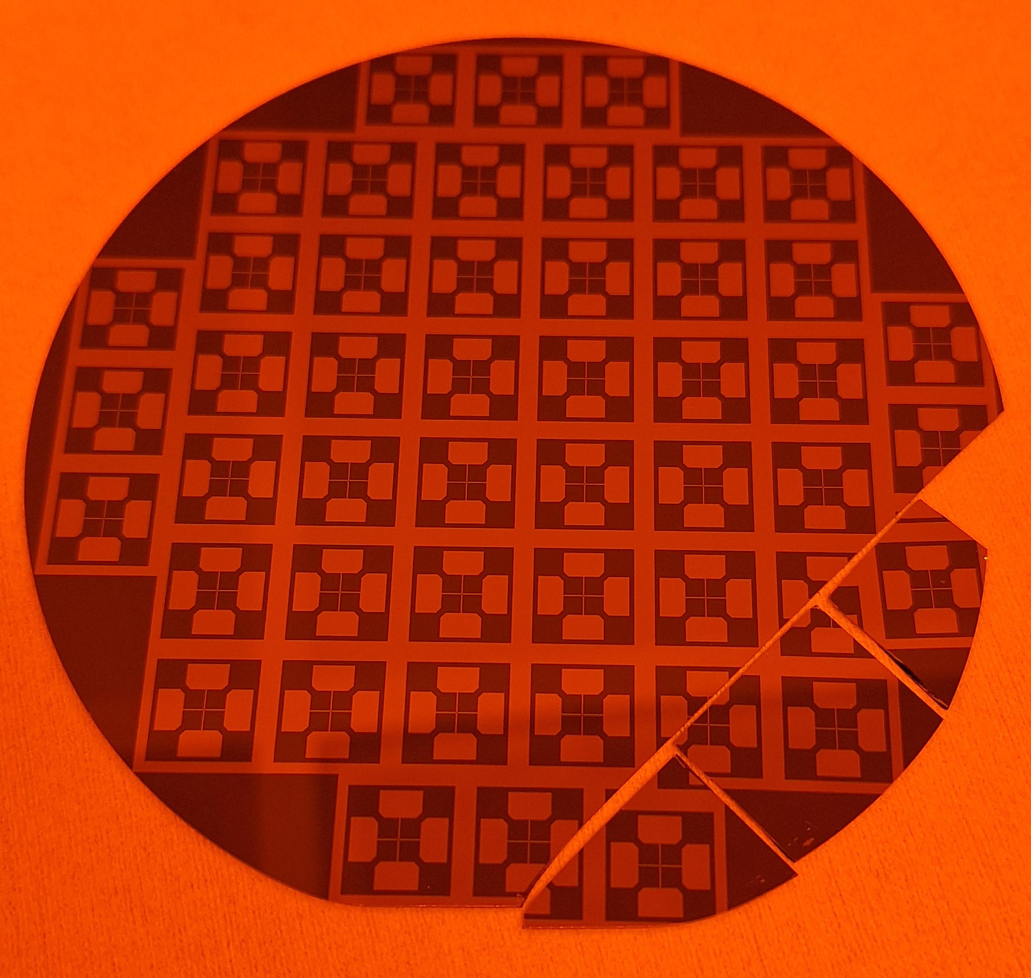
Cleaving Polysilicon Wafers
A senior laboratory services technician requested a quote for the following small quantity order.
Do you have any PolySilicon wafers? Two wafers , thickness can be > 1000 angstroms < 2000 angstroms.
Just on standard Si wafer <100> test wafer. Can be P-doped for n-type.
4” preferable if cheaper. Either way we are cleaving the wafer into multiple pieces.
UniversityWafer, Inc. Quoted:
Diameter 100mm SSP
Coating Poly Silicon wafers thickness > 1000 angstroms and <  2000 angstroms
Reference #320684 for specs and pricing.
Get Your Quote FAST! Or, Buy Online and Start Researching Today!
How to Cleave a Silicon Wafer
When cleaving silicon wafers, it is important to follow the correct Ori of the samples. For instance, if the sample is 60 degrees on one side, it must be cleaved along the 110 plane. The following are some tips to follow when chopping a silicon wafer. It is important to understand the correct Ori of the material. Also, if you are using the tool for semiconductor purposes, use a high-quality diamond scribe tip.
Please let us know if you have any questions or need instructions for silicon wafer cutting.
Video on How to Cleave Silicon Wafers.
Easy to Cut Silicon Wafer
How to cut silicon wafer? A scientist has asked the following question: We need 20 mm / 20 mm rectangular chips diced from naturally oxidized (100) (undoped) Si wafers, 400 microns thick. We need about 100 chips. We want to make sure that we can cleave them easily along a direction parallel to the rectangle sides, therefore the chips should be cut along the [100] directions. Can you please provide a quote? Just to confirm, the Si chips should be single-side polished and not be intentionally oxidized (just bare undoped Si, only naturally oxidized) which is very important for our application.
UniversityWafer, Inc. Quoted:
20mm x 20mm x 400um Chip, <100>, Undoped, SSP
Quantity: 100pcs
Ask for pricing.
Video: Cleaving (111) Silicon Wafers
Cleaving (111) Off-Cut Silicon Wafers
An adjunct professor requested a quote for the following:
I am looking for silicon that we will use it as a substrate when doing GI-XRD and get minimal signal from the substrate. I believe that {111} off cut silicon will do the trick. Do you have any prime grade silicon of the type that should work for my purposes?
Would we be able to cleave the silicon wafer into different pieces cleanly? Or would it break into several pieces due to it's Ori?
UniversityWafer, Inc. Quoted:
Generally, you can cleave all monocrystalline wafers. When stressed, such wafers break along cleavage planes.Cleavage planes are normally those presenting the highest surface density of atoms.
For face centered cubic structures like silicon, that is usually along (111) planes.Thus (510) wafers should cleave along intersections of (510) and (111) planes. There are two such directions on (510) wafers.
Since (510) is the same as (1, 0.2, 0), it is rather close to (100) so I expect (510) to cleave almost as neatly as (100) wafers.Still, it takes some skill to break wafers into neat rhombi.
You will shatter some wafers before you get the hang of it.
You may want to try your hand on inexpensive (100) wafers before you try it on more costly (510) wafers.
Reference RFQ#289995 for specs and pricing.
Cleaving Silicon Wafers
Micro-cleaving tools have been used to cleave silicon wafers for over 30 years. While they improved targeting  accuracy and sample quality, they were still limited by lower throughput, high cost, and inability to handle small samples. LatticeAx 420 is Electron Microscopy Sciences' highest-quality clive solution. It combines a small footprint workstation with a vision package and four-um optical resolution. This device enables cleaving with 10um accuracy in a matter of five minutes.
The standard process for cleaving silicon wafers produces dies with controlled dimensions and less material loss. Today, the thinnest cut of silicon is 200um. The quality of silicone wafers is crucial to the final product. The cleaving process directly affects the thickness and surface crystal Ori of the silicon. It is important to follow the process specifications, because any mistake can lead to uneven thickness, roughness, or loss of valuable materials.
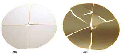
If for some reason you don't know if your wafers are (100) or (111) Ori, then you can use a hammer and nail to find out!
Cleaving (100) silicon wafers results on the left
Cleaving (111) silicon wafers
Watch the video above for cleaving instruction.
Let us know if you have any questions.
Researchers Experiment with CO2 Laser to Cleave Glass
In the experiment, researchers used a soda lime glass. We used a CO2 laser to cut the glass. After cutting, we observed the crack propagation using a high-speed polarization camera. The crack propagated as we expected. We measured the retardation of birefringence using a polarization camera and compared it with that of a numerical calculation. We also observed the retardation of birefringence at the crack tip. The retardation was consistent with that caused by mode I deformation. The mode I deformation decreased as the crack approached the edge of the glass.
What About Cleaving Germanium Wafers?
A researcher asks Do Germanium (100) wafers have cleavage planes? Dicing is not an option at the moment. Do cleavage planes for Germanium (100) essentially behave like Silicon (100), with cleavage planes being parallel to the major/minor flats (like you show in your left picture on your website, and in your weblink to the video on cleaving Si). Is that correct?
We already bought a (100) Germanium wafer from University Wafer earlier this summer (see forwarded email below). I just wanted to double-check with you before making a cleaving attempt. I'm very comfortable cleaving with GaAs/InP/Si etc, but I have not yet tried Ge wafers.
Researcher purchased
Ge Item #2478
50.8mm Undoped <100> >50 ohm-cm 500um SSP
UniversityWafer, Inc. Replied:
The difference between cleaving Silicon vs Germanium wafers is that you have to dice by machine. Simply cleaving will not provide good results as Ge are more brittle than Si.
What Cleaved Silicon Wafers are Used for: Elastocapillary Interactions Between Liquids and Thin Solid Films Under Tension Research?
Research Paper
In addition, primarily two materials were used as substrates. Silicon wafers (UniversityWafer) were cleaved into 1 cm x 1 cm pieces to serve as a supporting rigid
substrate for polymer �lms. Freshly cleaved 3 cm x 3 cm mica substrates were used solely as an intermediary for �lms that were to be strained or made free-standing, as will be described in more detail in the following section. Silicon and mica are ideal substrates because they are extremely smooth and clean when freshly
cleaved.
You may know, our group decided to purchase one double side polished wafer on the website and received the order yesterday. First of all thanks for your assist on this purchase!
How to Cleave Silicon Wafers if The Orienation is Unkown?
A Materials Science and Engineering student requested help with the following cleaving issue:
I am writing to ask a question on a Si wafer. I’ve recently read an article using a product from your company and am wondering if this product is still available. Below is a description that I found from the article. “A p-type Si(100) wafer (UniversityWafer) of 5−10 Ω-cm resistivity and 100 μm thickness was cut into 25.4 mm × 25.4 mm pieces, which were double-polished, thoroughly cleaned, and then used both as IR transport window and working electrode.
We would like to cleave the wafer and realize that this wafer is in a circular shape without any guide of Ori. We are wondering if you can give us some suggestions / advice on cleaving this Si.
UniversityWafer, Inc. Replied. Reference #276466 for more.
Certainly! Cleaving a silicon (Si) wafer without a clear Ori can be a bit tricky, but not impossible. Here are some steps and suggestions to help you cleave your circular Si wafer:
-
Safety First: Always wear safety glasses and gloves when handling wafers.
-
Clean Surface: Ensure that the wafer surface is clean and free from dust or other contaminants.
-
Score the Wafer:
- Using a diamond scribe, lightly score the wafer surface along the desired cleave line. If you don't have a defined cleave line because of the lack of Ori markers, just decide on the direction you want. Silicon wafers usually cleave easiest along the crystal planes, so if you can identify or guess the Ori, it can be beneficial.
- Hold the wafer with the score mark facing upward, placing it between your thumbs with the score mark under one of the thumbs. Make sure the wafer is well-supported; you don't want it to break in the wrong place or drop it.
-
Cleaving:
- Using gentle but increasing pressure, press down and outwards with your thumbs to initiate the cleave. The cleave should propagate along the score mark.
- If it doesn’t cleave immediately, try flexing the wafer very slightly along the score line.
-
Multiple Cleave Lines:
- If you want smaller pieces, repeat the scoring and cleaving process in the desired direction.
-
Post-Cleaving:
- Inspect the cleaved surfaces for any irregularities or chipping.
- Store or handle the cleaved wafer pieces carefully to avoid any damage or contamination.
-
Alternative Methods:
- There are automated wafer cleaving tools available in the market, which might provide more uniform and precise cleaving, especially for wafers without Ori markers. If you have access to these tools, they can be a great alternative.
-
Identification of Crystallographic Ori:
- While not immediately useful if your wafer lacks an Ori flat or notch, for future reference, it might be helpful to get oriented wafers or learn to identify the Ori. This can make cleaving much easier and predictable.
- Silicon wafers often cleave more cleanly along certain crystallographic planes (typically {100} or {110}). Knowing these planes or having wafers with Ori markers can assist in getting clean cleaved edges.
In conclusion, while cleaving an unoriented wafer can be a bit of a challenge, with care and the right technique, you can achieve relatively clean and straight breaks. If you consistently work with Si wafers, it might be worth investing in automated cleaving equipment or ensuring you get wafers with clear Ori guides in the future.
