
Thermal Oxide Silicon Wafers for Research
UniversityWafer supplies thermal oxide silicon wafers for semiconductor fabrication, MEMS, photonics, materials science, and university research. The silicon dioxide (SiO2) layer is thermally grown directly from the silicon substrate, providing a stable dielectric surface for a wide variety of experiments and device structures.
Researchers can select silicon wafers based on diameter, crystal orientation, conductivity type, resistivity, thickness, surface finish, and required thermal oxide thickness.
Benefits of Thermally Grown SiO2
Thermal oxidation provides a high-quality Si-SiO2 interface that has made silicon dioxide an important material in semiconductor research and fabrication. Depending on the process requirements, wet or dry thermal oxidation can be used to produce different oxide thicknesses.
- Excellent electrical insulation and dielectric properties
- High-quality Si-SiO2 interface
- Useful for surface passivation and device isolation
- Suitable for photolithography and masking experiments
- Compatible with many thin-film deposition processes
- Available for a wide range of research applications
Applications of Thermal Oxide Wafers
Thermally oxidized silicon substrates are widely used as starting materials and experimental platforms. Typical applications include:
- Semiconductor device development
- Gate dielectric and electrical characterization studies
- MEMS fabrication and process development
- Thin-film deposition and characterization
- Photolithography and etching experiments
- Surface functionalization and sensor research
- Photonics and optical research
- University teaching and laboratory experiments
Wet and Dry Oxide for Different Research Needs
Dry oxidation generally offers slower, more controlled oxide growth and is commonly selected when relatively thin, high-quality oxide layers are required. Wet oxidation provides a faster growth rate and is useful when thicker SiO2 layers are needed.
The appropriate process and oxide thickness depend on the intended application. Researchers can learn more about thermal oxide deposition on silicon wafers and available substrate options.
Specify Your Thermal Oxide Wafer
When requesting thermally oxidized wafers, consider the silicon wafer diameter, orientation, resistivity, conductivity type, wafer thickness, surface finish, oxide thickness, and whether SiO2 is needed on one or both wafer surfaces.
Need Thermal Oxide Silicon Wafers?
Tell us your wafer and SiO2 specifications, quantity, and research requirements. UniversityWafer can help you source oxidized silicon substrates for your application.
Get Your Thermal Oxide Wafer Quote FAST! Or, Buy Online and Start Researching Today!
What Is Thermal Oxide on Silicon?
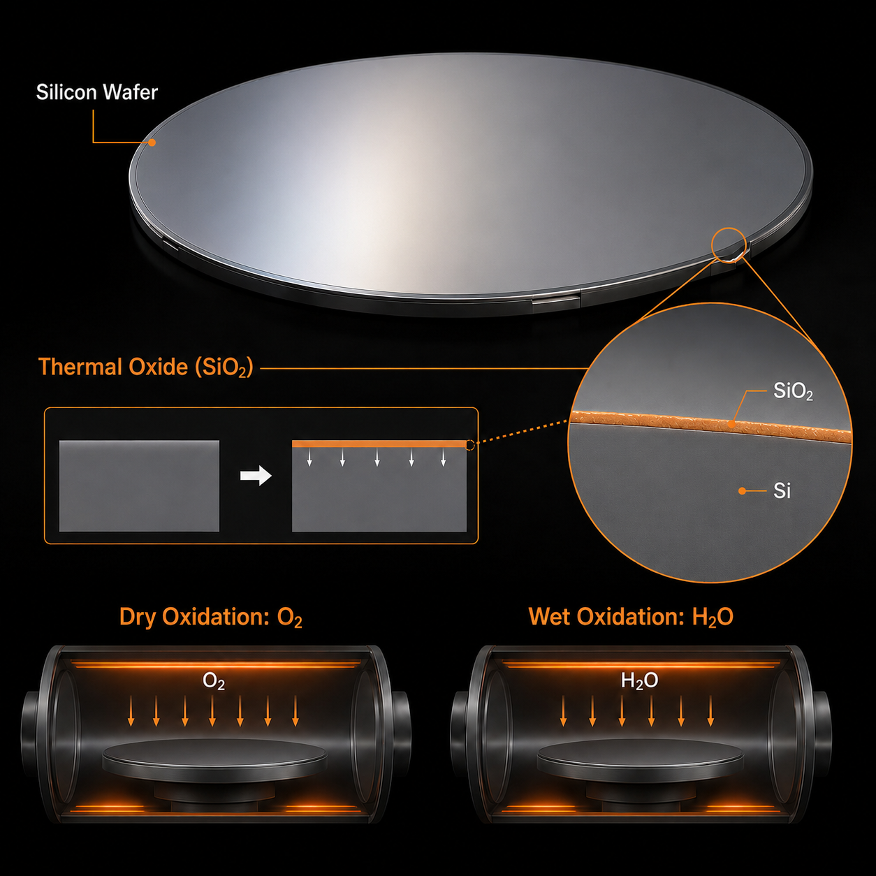
Thermal oxide is a silicon dioxide (SiO2) layer formed by exposing a silicon wafer to an oxidizing environment at elevated temperature. Unlike a deposited SiO2 film, thermal oxidation consumes part of the silicon surface as the oxide grows, producing a Si-SiO2 interface valued for many semiconductor and research applications.
Wet vs. Dry Thermal Oxidation
The two primary processes used to grow thermal oxide are wet oxidation and dry oxidation. The appropriate method depends on the desired oxide thickness, growth rate, and application.
| Property | Dry Oxidation | Wet Oxidation |
|---|---|---|
| Oxidant | Oxygen (O2) | Water vapor (H2O) |
| Growth Rate | Slower | Faster |
| Typical Use | Thin, high-quality oxide layers | Thicker oxide layers |
| Common Applications | Gate dielectrics, electronic research | Isolation, masking, MEMS and research |
Why Use SiO2 on Silicon Wafers?
Silicon dioxide is an important dielectric material in semiconductor technology. A controlled SiO2 layer can provide electrical insulation, surface passivation, masking, and device isolation while also serving as a useful platform for fabrication and materials research.
Thermally oxidized wafers are commonly used for:
- Semiconductor device fabrication
- Electrical and dielectric research
- MEMS research
- Thin-film deposition experiments
- Surface modification and functionalization
- Photolithography and process development
- Optical and photonics research
- Device isolation and passivation studies
Thermal Oxide Thickness
The required thermal oxide thickness depends on the experiment or device design. Thin oxides can be useful for dielectric and electronic studies, while thicker SiO2 layers are frequently selected for electrical isolation, optical structures, masking, and MEMS applications.
Researchers should consider oxide thickness, wafer diameter, silicon crystal orientation, resistivity, surface finish, and whether oxide is required on one or both sides when specifying an oxidized wafer.
Thermal Oxide Wafers for Research
UniversityWafer supplies thermal oxide silicon wafers for university, laboratory, semiconductor, MEMS, and materials-science applications. Silicon substrates can be specified with different wafer diameters, orientations, resistivities, thicknesses, and oxide requirements to support a wide range of experimental needs.