
Professional Silicon Wafer Surface Cleaning Solutions
Successful semiconductor fabrication begins with a clean substrate. Contaminants such as dust particles, organic residues, metallic impurities, and native silicon oxide can significantly reduce device performance and manufacturing yield. UniversityWafer supplies premium silicon wafers and provides wafer processing services to help researchers and manufacturers achieve contamination-free surfaces for advanced applications.
Whether preparing wafers for photolithography, thermal oxidation, thin-film deposition, epitaxial growth, or wafer bonding, selecting the proper cleaning method is essential. Our technical resources cover industry-standard cleaning techniques such as RCA SC-1, RCA SC-2, hydrofluoric acid (HF) oxide removal, piranha cleaning, solvent cleaning, plasma cleaning, and UV-ozone treatment used throughout semiconductor manufacturing.
Benefits of Proper Wafer Surface Preparation
- Removes particles, organic residues, and metallic contamination
- Improves thin-film adhesion and coating uniformity
- Enhances photolithography accuracy
- Produces cleaner oxide and epitaxial layers
- Reduces surface defects and wafer contamination
- Increases semiconductor device yield and reliability
- Supports high-performance MEMS, photonics, and microelectronics fabrication
Applications of Clean Silicon Wafers
Properly cleaned silicon wafers are used throughout the semiconductor industry and research laboratories for manufacturing integrated circuits, MEMS devices, power electronics, biosensors, photonic components, solar cells, RF devices, and advanced microelectronic systems. High-quality surface preparation is essential before oxidation, diffusion, ion implantation, ALD, CVD, PVD, and other wafer processing steps.
Get Your Silicon Wafer Quote FAST!
Need clean, research-grade silicon wafers or custom wafer processing? Request a Quote or Buy Online and start your research today!
Why Is Silicon Wafer Surface Cleaning Important?
Silicon wafer surface cleaning is one of the most critical steps in semiconductor manufacturing. Even microscopic particles, organic residues, metallic contaminants, or native oxide layers can negatively affect photolithography, thin-film deposition, oxidation, epitaxial growth, and device performance. Proper cleaning ensures a contamination-free surface that improves film adhesion, electrical reliability, and fabrication yield.
Whether producing integrated circuits, MEMS devices, photonic components, sensors, or power electronics, selecting the appropriate cleaning process helps maintain consistent wafer quality throughout fabrication.
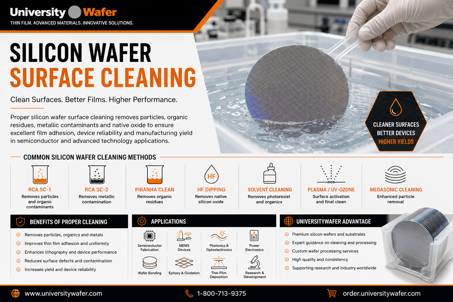
Common Silicon Wafer Cleaning Methods
- RCA SC-1 Cleaning – Removes particles and organic contaminants using ammonium hydroxide, hydrogen peroxide, and deionized water.
- RCA SC-2 Cleaning – Eliminates metallic contamination using hydrochloric acid, hydrogen peroxide, and deionized water.
- Piranha Cleaning – Uses sulfuric acid and hydrogen peroxide to remove heavy organic residues from wafer surfaces.
- HF (Hydrofluoric Acid) Dip – Removes native silicon dioxide prior to oxidation, epitaxy, or thin-film deposition.
- Solvent Cleaning – Acetone, isopropyl alcohol (IPA), and other solvents remove photoresist and organic contaminants.
- Plasma & UV-Ozone Cleaning – Effective for final surface activation before bonding or thin-film deposition.
Applications Requiring Ultra-Clean Silicon Surfaces
Clean silicon wafers are required for numerous advanced research and manufacturing processes, including:
- Semiconductor device fabrication
- Photolithography
- Thermal oxidation
- Silicon epitaxy
- ALD, CVD, and PVD thin-film deposition
- MEMS fabrication
- Wafer bonding
- Microelectronics packaging
- Photonics and optical devices
- University and industrial research
UniversityWafer Wafer Processing Services
UniversityWafer supplies premium silicon wafers and offers professional wafer processing services, including precision cleaning, polishing, thermal oxidation, silicon nitride deposition, dicing, lapping, and custom substrate preparation. Our processing capabilities help researchers and manufacturers obtain clean, high-quality wafer surfaces ready for advanced semiconductor fabrication.