
Custom Thermal Oxide Silicon Wafer Solutions
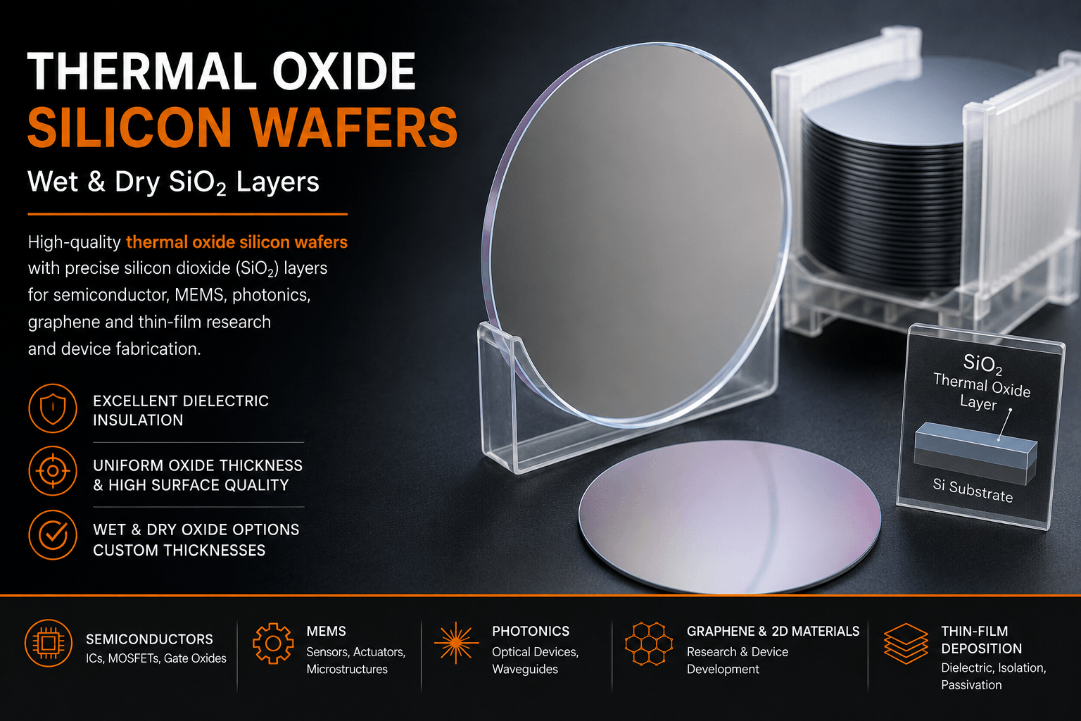
UniversityWafer supplies high-quality thermal oxide silicon wafers with precision-grown silicon dioxide (SiO2) layers for semiconductor manufacturing, university research, MEMS fabrication, and advanced photonic devices. Whether you require a few prototype wafers or production quantities, we can provide thermal oxide substrates manufactured to your exact specifications.
Our thermal oxide deposition process produces dense, uniform oxide layers with excellent electrical insulation and surface quality. Customers can choose between wet thermal oxide for thicker oxide layers or dry thermal oxide for thinner, high-quality dielectric films depending on their application requirements.
Available Specifications
- Custom oxide thicknesses
- Wet and dry thermal oxidation
- Single-side or double-side polished silicon
- <100>, <111>, and <110> crystal orientations
- P-type and N-type silicon
- Prime and test grade wafers
- Standard and custom wafer diameters
- Research through production quantities
Common Applications
- MEMS fabrication
- Photonics
- Thin-film deposition
- Graphene research
- Semiconductor device fabrication
- Dielectric isolation
- Surface passivation
- University and industrial R&D
Recent Research Inquiry
"We require 100 mm <100> silicon wafers with a 500 nm dry thermal oxide layer for MEMS sensor fabrication. Can you provide prime-grade wafers with tight oxide thickness tolerance and double-side polishing?"
Our engineering team can recommend the optimal oxide process, wafer orientation, resistivity, and oxide thickness for your specific research or production requirements.
Get Your Thermal Oxide Silicon Wafer Quote FAST! Or Buy Online and Start Researching Today!
What Is Thermal Oxide Deposition?
Thermal oxide deposition, more accurately known as thermal oxidation, is a process that grows a high-quality layer of silicon dioxide (SiO2) directly on the surface of a silicon wafer. Unlike deposited oxide films produced by CVD or PECVD, thermal oxide is created by exposing silicon to oxygen or water vapor at elevated temperatures, causing the silicon itself to react and form a dense, electrically insulating oxide layer. This process produces exceptional interface quality, excellent thickness uniformity, and superior electrical performance for advanced semiconductor devices.
UniversityWafer supplies thermal oxide silicon wafers with custom oxide thicknesses for research, prototype development, and production applications. Wet and dry oxidation processes are available depending on your required dielectric properties and oxide thickness.
Wet vs. Dry Thermal Oxide
The two primary thermal oxidation methods each provide distinct advantages depending on the intended application.
| Oxidation Process | Advantages | Typical Applications |
|---|---|---|
| Dry Thermal Oxide | Dense oxide, superior electrical properties, precise thickness control | Gate oxides, MOS devices, high-performance integrated circuits |
| Wet Thermal Oxide | Faster growth rate and thicker oxide layers | MEMS, dielectric isolation, masking, field oxide, passivation |
Advantages of Thermal Oxide Silicon Wafers
Compared with deposited dielectric films, thermal oxide silicon wafers offer outstanding electrical insulation, excellent adhesion, and highly uniform oxide thickness. These characteristics make them one of the most widely used substrates in semiconductor fabrication and university research.
- Excellent dielectric insulation
- High-quality Si/SiO2 interface
- Superior oxide thickness uniformity
- Excellent chemical stability
- Outstanding adhesion to silicon
- Available in custom oxide thicknesses
- Compatible with advanced lithography and microfabrication
- Ideal for research and production environments
Common Applications
Thermally oxidized silicon wafers are used throughout the semiconductor industry and scientific research because they provide reliable electrical isolation and an ideal surface for device fabrication.
- MEMS fabrication
- Photonic devices
- Graphene and 2D materials research
- Thin-film deposition
- Photolithography
- Semiconductor device fabrication
- Surface passivation
- Integrated circuits and sensors
Thermal Oxide Compared with Other Silicon Wafer Types
| Wafer Type | Primary Advantage | Typical Applications |
|---|---|---|
| Thermal Oxide Silicon | High-quality SiO2 dielectric layer | MEMS, ICs, sensors, semiconductor fabrication |
| SOI Wafers | Buried oxide for improved device isolation | MEMS, RF, CMOS, power electronics |
| Silicon Nitride Wafers | Excellent diffusion barrier and passivation layer | MEMS, semiconductor processing, masking |
| Bare Silicon Wafers | General-purpose semiconductor substrate | Microelectronics, photonics, research |
| Silicon-on-Insulator (SOI) | Excellent electrical isolation and reduced parasitic capacitance | Advanced CMOS, MEMS, RF devices |