Silicon-on-Insulator (SOI) Wafers for MEMS, RF & Advanced Semiconductor Devices
UniversityWafer supplies high-quality Silicon-on-Insulator (SOI) wafers for MEMS, RF electronics, silicon photonics, CMOS devices, power electronics, and advanced semiconductor research. We offer custom SOI substrates with configurable device-layer thickness, buried oxide (BOX), handle wafer properties, crystal orientation, resistivity, and surface finish to support both prototype development and high-volume manufacturing.
Need Custom Silicon-on-Insulator (SOI) Wafers?
UniversityWafer, Inc. supplies premium Silicon-on-Insulator (SOI) wafers for universities, research laboratories, semiconductor foundries, and technology companies worldwide. Our SOI substrates are engineered for high-performance applications including MEMS, RF electronics, silicon photonics, power devices, sensors, and advanced integrated circuits.
Whether you require standard SOI wafers or fully customized specifications, our team can provide the device layer, buried oxide (BOX), handle wafer, crystal orientation, resistivity, thickness, and surface finish needed for your research or production project.
Typical SOI Wafer Specifications
- Device layer thickness from ultra-thin to several microns
- Custom buried oxide (BOX) thickness
- Standard silicon handle wafers
- <100>, <111>, and other crystal orientations
- P-type, N-type, intrinsic, and custom resistivity options
- Single-Side Polished (SSP) or Double-Side Polished (DSP)
- Epi-ready surface finishes available
- Research and production wafer diameters
Applications of SOI Wafers
Silicon-on-insulator technology improves device performance by reducing parasitic capacitance, minimizing electrical leakage, and enhancing switching speed. As a result, SOI wafers are widely used in numerous semiconductor applications, including:
- MEMS sensors and actuators
- RF switches and RF front-end devices
- Silicon photonics
- Power integrated circuits
- CMOS and FD-SOI technologies
- Microprocessors and low-power electronics
- Biomedical sensors
- Advanced semiconductor research
Request Your SOI Wafer Quote
Complete the quotation request form with your required SOI wafer specifications, including device-layer thickness, buried oxide thickness, handle wafer properties, orientation, resistivity, diameter, and quantity. Our technical team will provide a fast quotation and help you select the optimal SOI substrate for your application.
Get Your Silicon-on-Insulator (SOI) Wafer Quote FAST! Or Buy Online and Start Researching Today!
What Is a Silicon-on-Insulator (SOI) Wafer?
A Silicon-on-Insulator (SOI) wafer is a specialized semiconductor substrate consisting of three layers: a thin silicon device layer, a buried oxide (BOX) insulating layer, and a silicon handle wafer. By electrically isolating the active devices from the substrate, SOI technology reduces parasitic capacitance, lowers power consumption, and improves switching speed compared to conventional bulk silicon wafers.
SOI wafers are widely used in advanced semiconductor manufacturing for MEMS, RF devices, silicon photonics, CMOS integrated circuits, sensors, and power electronics where high performance and improved reliability are required.
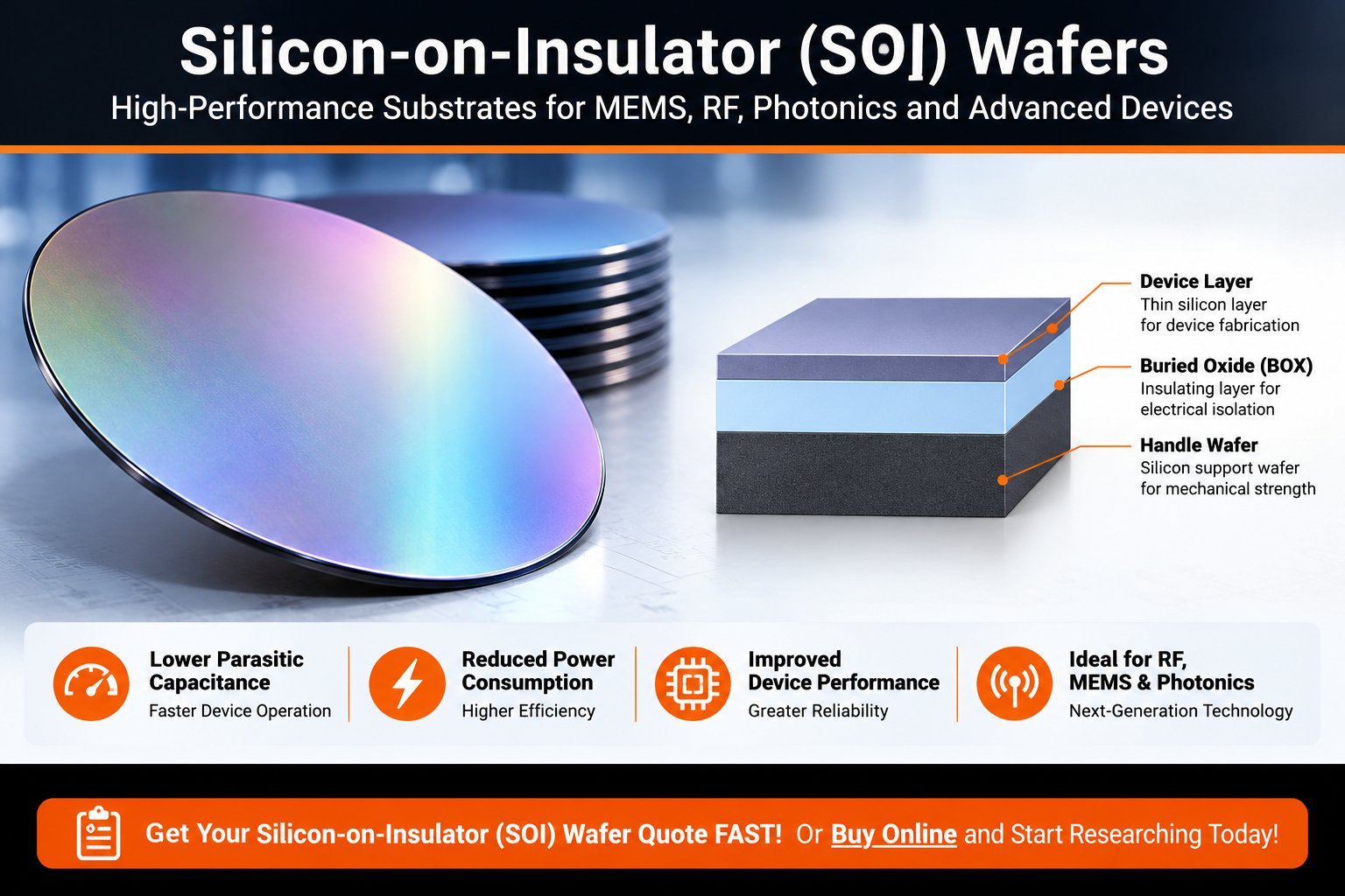
Structure of an SOI Wafer
Each Silicon-on-Insulator wafer is engineered with three functional layers that work together to optimize electrical performance and device isolation.
| Layer |
Purpose |
| Device Layer |
Thin monocrystalline silicon used to fabricate transistors, MEMS structures, photonic devices, and integrated circuits. |
| Buried Oxide (BOX) |
Silicon dioxide insulating layer that electrically isolates the device layer from the substrate, reducing leakage current and parasitic capacitance. |
| Handle Wafer |
Mechanical support wafer that provides structural strength during processing and device fabrication. |
Advantages of Silicon-on-Insulator Technology
- Lower parasitic capacitance for faster device operation
- Reduced power consumption
- Lower leakage currents
- Improved radiation hardness for aerospace and defense applications
- Higher operating frequencies for RF electronics
- Excellent thermal and electrical isolation
- Improved device reliability and performance
- Compatible with advanced CMOS manufacturing processes
Available SOI Wafer Options
UniversityWafer supplies Silicon-on-Insulator wafers with numerous configurable specifications to meet research and production requirements.
- Ultra-thin and standard device-layer thicknesses
- Custom buried oxide (BOX) thicknesses
- P-type, N-type, and intrinsic silicon
- <100>, <111>, and custom crystal orientations
- Single-Side Polished (SSP) and Double-Side Polished (DSP)
- Epi-ready surface finishes
- Research and production wafer diameters
- Custom resistivity, thickness, and tolerance specifications
Common Applications of SOI Wafers
Silicon-on-Insulator technology is used across many of today's fastest-growing semiconductor markets because it enables higher performance while reducing power consumption.
- MEMS sensors and accelerometers
- RF switches and RF front-end modules
- Silicon photonics and optical communications
- CMOS and FD-SOI integrated circuits
- Power management ICs
- Automotive electronics
- Biomedical and microfluidic devices
- Quantum computing research
- High-speed processors
- University and government semiconductor research
Why Choose SOI Wafers?
Compared to conventional bulk silicon, Silicon-on-Insulator wafers offer improved electrical isolation, lower power consumption, faster switching speeds, and enhanced device performance. These advantages make SOI substrates an excellent choice for next-generation MEMS, RF electronics, photonics, and advanced semiconductor devices where efficiency and reliability are critical.
Related SOI & Semiconductor Resources
