Thermal Oxide Silicon Wafers
Thermal oxide silicon wafers feature a precisely grown layer of
silicon dioxide (SiO2) that provides excellent electrical
insulation, surface passivation, and dielectric performance. UniversityWafer
supplies wet and dry thermal oxide wafers with custom oxide
thicknesses, wafer diameters, crystal orientations, and dopant options for
MEMS, CMOS, photolithography, wafer bonding, and advanced semiconductor
research.
Get Your Thermal Oxide Wafer Quote FAST!
UniversityWafer supplies high-quality thermal oxide silicon wafers
for semiconductor fabrication, MEMS, photonics, microelectronics, and advanced
materials research. Whether you require wet thermal oxide,
dry thermal oxide, or a custom silicon dioxide (SiO2)
layer, our engineers can help you select the right wafer for your application.
We offer thermal oxide wafers in a wide range of diameters, crystal
orientations, oxide thicknesses, dopant types, resistivities, and surface
finishes. Standard inventory and custom specifications are available for both
prototype and production quantities.
Recent Research Inquiry
"Our research group is fabricating MEMS pressure sensors and requires
100 mm silicon wafers with a
1 µm dry thermal oxide layer, (100) orientation,
single-side polished, and low particle density. Could you provide pricing,
availability, and lead time for an initial prototype order?"
Custom Thermal Oxide Wafer Options
- Wet and dry thermal oxide growth
- Custom SiO2 thicknesses from thin gate oxides to thick dielectric layers
- 2", 3", 4", 6", 8", and 12" wafer diameters
- (100), (111), and custom crystal orientations
- N-type, P-type, and intrinsic silicon substrates
- Prime, test, and research grades
- Single-side polished (SSP) and double-side polished (DSP)
- Prototype through high-volume production quantities
Complete the quote request form with your desired wafer diameter, oxide
thickness, crystal orientation, resistivity, polish, and quantity. Our
technical team will respond quickly with pricing and recommendations for your
thermal oxide wafer project.
Get Your Quote FAST! Or,
Buy Online
and Start Researching Today!
What Are Thermal Oxide Silicon Wafers?
Thermal oxide silicon wafers are silicon substrates coated
with a layer of high-quality silicon dioxide (SiO2)
grown through thermal oxidation. This process produces an electrically
insulating oxide with excellent interface quality, making thermal oxide wafers
an essential material for semiconductor manufacturing, MEMS devices,
microelectronics, photonics, biosensors, and advanced materials research.
Depending on the application, the oxide layer can be grown using either
dry oxidation or wet oxidation, each offering
distinct advantages in oxide quality, growth rate, and electrical performance.
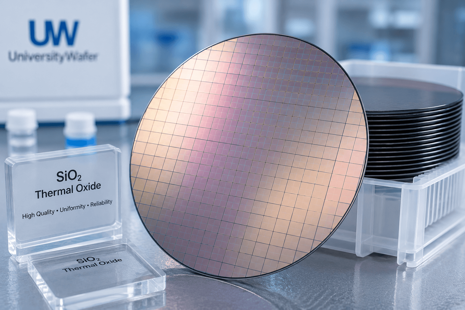
Wet vs. Dry Thermal Oxide
| Process |
Characteristics |
Typical Applications |
| Dry Thermal Oxide |
Dense, high-quality SiO2 with excellent electrical properties and precise thickness control. |
Gate oxides, MOS devices, CMOS fabrication, dielectric layers. |
| Wet Thermal Oxide |
Faster oxide growth for thicker films with excellent insulation properties. |
MEMS, field oxides, diffusion masking, surface passivation. |
Applications of Thermal Oxide Wafers
Because thermal oxide provides outstanding electrical insulation and chemical
stability, these wafers are widely used throughout the semiconductor industry
and research laboratories.
- CMOS and MOSFET fabrication
- MEMS sensors and actuators
- Photolithography masking layers
- Wafer bonding processes
- Microfluidic and biosensor devices
- Thin-film deposition substrates
- Graphene and other 2D material research
- Photonic integrated circuits
- Dielectric isolation layers
- University and government laboratory research
Available Thermal Oxide Wafer Specifications
UniversityWafer supplies thermal oxide silicon wafers with
customizable specifications to support both research and commercial
manufacturing. Standard and custom options include:
- 2", 3", 4", 6", 8", and 12" wafer diameters
- Custom oxide thicknesses from thin gate oxides to thick dielectric layers
- (100), (111), and custom crystal orientations
- N-type, P-type, and intrinsic silicon substrates
- Prime, test, and research grades
- Single-side polished (SSP) and double-side polished (DSP)
- Low particle, low TTV, and high-flatness options
- Prototype through production quantities
Custom Thermal Oxide Solutions
Whether you require ultra-thin gate oxides for advanced semiconductor devices
or thick oxide layers for MEMS fabrication and dielectric isolation,
UniversityWafer can provide custom thermal oxide wafers
manufactured to your exact specifications. Our engineering team supports
universities, research institutes, and semiconductor manufacturers with
high-quality wafers designed to meet demanding process and performance
requirements.
Related Resources
