
What Is Molecular Beam Epitaxy (MBE)?
Molecular Beam Epitaxy (MBE) is an advanced epitaxial growth technique used to deposit highly controlled crystalline layers onto semiconductor substrates. The process takes place under ultra-high-vacuum (UHV) conditions, allowing beams of atoms or molecules to travel toward a heated substrate with minimal interaction with background gases.
When the incoming species reach the substrate surface, they can migrate across the surface and incorporate into the growing crystal lattice. Carefully controlled growth conditions allow researchers to fabricate epitaxial thin films with precise composition, doping, interfaces, and layer thicknesses.
How Does Molecular Beam Epitaxy Work?
Inside an MBE system, source materials are typically heated in specialized effusion cells or other sources to generate beams of constituent species. These beams are directed toward a heated semiconductor wafer positioned inside the vacuum chamber.
Individual sources can be controlled with shutters, allowing researchers to start or stop the arrival of particular elements during growth. This precise control makes it possible to create complex multilayer structures and abrupt interfaces between different semiconductor materials.
Basic MBE Growth Process
- Substrate preparation – The wafer surface is prepared to provide a clean crystalline template for epitaxial growth.
- Ultra-high vacuum – The growth chamber is maintained at extremely low pressure to minimize contamination and unwanted gas-phase interactions.
- Source evaporation – Selected materials are heated to generate atomic or molecular beams.
- Beam control – Mechanical shutters regulate which source materials reach the substrate and when.
- Epitaxial growth – Incoming species interact with the heated substrate surface and become incorporated into the growing crystalline layer.
- In-situ monitoring – Techniques such as RHEED may be used to observe surface structure and growth behavior during deposition.
Why Use MBE for Semiconductor Research?
One of the primary advantages of MBE is its exceptional degree of control over epitaxial layer growth. Relatively slow deposition rates and independently controlled material sources allow researchers to engineer semiconductor structures at extremely small length scales.
MBE is particularly valuable when a research project requires carefully controlled interfaces or sophisticated sequences of materials that would be difficult to produce using less precise deposition methods.
Key Advantages of MBE
- Precise thickness control – Enables growth of extremely thin semiconductor layers.
- Sharp interfaces – Useful for fabricating multilayer heterostructures and quantum structures.
- Composition control – Multiple sources can be independently adjusted to engineer semiconductor alloys.
- Controlled doping – Dopant sources can be incorporated during epitaxial growth.
- High-purity environment – Ultra-high vacuum helps reduce contamination during deposition.
- In-situ characterization – Surface-sensitive techniques can monitor growth without removing the wafer from the vacuum environment.
Semiconductor Materials Grown by MBE
MBE can be used to investigate a wide range of semiconductor material systems. It is especially important for III-V compound semiconductors, where precise control over composition and heterointerfaces enables advanced electronic and optoelectronic structures.
Materials commonly associated with MBE research include:
- Gallium arsenide (GaAs)
- Aluminum gallium arsenide (AlGaAs)
- Indium arsenide (InAs)
- Indium phosphide (InP)
- Indium gallium arsenide (InGaAs)
- Gallium nitride (GaN)
- Aluminum gallium nitride (AlGaN)
- Silicon (Si)
- Germanium (Ge)
- Silicon-germanium (SiGe)
MBE Substrate Selection
Selecting the appropriate substrate is critical for successful epitaxial growth. Researchers must consider lattice matching, crystal orientation, surface preparation, thermal properties, substrate quality, and compatibility between the wafer and the material being deposited.
For example, gallium arsenide wafers are widely used as substrates for III-V epitaxial research, while silicon wafers provide an important platform for silicon-based epitaxy, heterostructures, and advanced semiconductor research.
Important MBE Wafer Specifications
- Substrate material
- Crystal orientation
- Wafer diameter and thickness
- Surface finish
- Miscut or off-axis orientation
- Dopant type and concentration
- Electrical resistivity
- Surface cleanliness
- Crystal and defect quality
Applications of Molecular Beam Epitaxy
The ability to precisely engineer semiconductor layers makes MBE valuable across electronics, photonics, optoelectronics, quantum research, and advanced materials development.
- Quantum wells and quantum dots
- Semiconductor superlattices
- III-V heterostructures
- High-electron-mobility transistors (HEMTs)
- Laser diodes
- Photodetectors
- LED research
- Solar cells and photovoltaic structures
- Infrared devices
- Quantum electronic devices
- Advanced semiconductor material research
Get Your MBE Substrate Quote FAST!
Or, Buy Wafers Online and Start Researching Today!
MBE vs. Other Epitaxial Growth Methods
Molecular Beam Epitaxy is one of several techniques used to grow crystalline semiconductor layers. Other approaches include chemical vapor deposition (CVD), metal-organic chemical vapor deposition (MOCVD), and various forms of vapor-phase epitaxy.
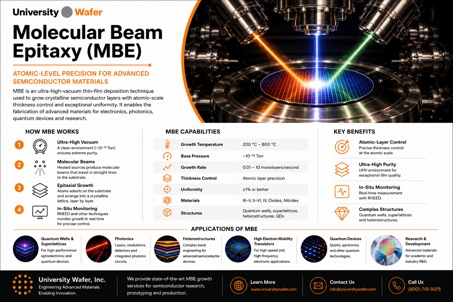
MBE is distinguished by its ultra-high-vacuum environment, independently controlled material sources, relatively slow growth rates, and precise interface control. These characteristics make it particularly useful for research involving extremely thin layers and complex semiconductor heterostructures.
| Characteristic | MBE | MOCVD |
|---|---|---|
| Growth Environment | Ultra-high vacuum | Controlled gas-phase reactor |
| Material Delivery | Atomic or molecular beams | Metal-organic and hydride precursors |
| Growth Rate | Typically relatively slow | Generally faster |
| Interface Control | Excellent | Excellent with optimized processes |
| In-Situ Monitoring | RHEED commonly used | Optical and other monitoring methods |
| Typical Applications | Quantum structures, heterostructures and research | LEDs, lasers, power electronics and production epitaxy |
What Is RHEED in Molecular Beam Epitaxy?
Reflection High-Energy Electron Diffraction (RHEED) is an in-situ characterization technique frequently associated with MBE systems. A beam of high-energy electrons strikes the substrate surface at a shallow angle, producing a diffraction pattern that provides information about the crystalline surface.
Researchers can use RHEED to study surface reconstruction, crystal quality, growth behavior, and epitaxial layer development without removing the wafer from the MBE chamber. Under suitable growth conditions, RHEED intensity oscillations can also provide information useful for monitoring growth rates.
MBE for Quantum Wells and Superlattices
One of the major research advantages of MBE is its ability to produce extremely thin alternating semiconductor layers. This makes the technique particularly valuable for creating quantum wells, superlattices, and other quantum-confined structures.
A quantum well can be formed by placing a thin semiconductor layer between materials with different bandgaps. When the active layer becomes sufficiently thin, charge carriers can experience quantum confinement, producing electronic and optical properties that differ from those of the bulk material.
Repeating multiple layers with carefully selected thicknesses and compositions can produce a semiconductor superlattice. These structures are investigated for infrared detectors, lasers, quantum devices, high-speed electronics, and fundamental semiconductor physics.
MBE for Semiconductor Heterostructures
A heterostructure is created when layers of different semiconductor materials are combined within the same device. MBE provides researchers with precise control over the transition from one material composition to another, making it particularly useful for engineering complex heterointerfaces.
Common III-V combinations include GaAs with AlGaAs , as well as InGaAs, InAs, InP, and related compound-semiconductor systems.
MBE for High-Electron-Mobility Transistors
High-electron-mobility transistors (HEMTs) use semiconductor heterostructures to create channels capable of supporting high carrier mobility. Precise epitaxial control is important because the electrical behavior of the device depends strongly on layer composition, thickness, doping, and interface quality.
MBE can be used to grow experimental structures for high-frequency electronics, RF devices, microwave systems, low-noise electronics, and advanced transistor research.
MBE for Photonics and Optoelectronics
Molecular Beam Epitaxy is also important for creating semiconductor structures that interact with light. By controlling bandgap, composition, and layer thickness, researchers can engineer materials for specific optical wavelengths and device functions.
MBE-grown structures are investigated for:
- Laser diodes
- Light-emitting diodes (LEDs)
- Photodetectors
- Infrared detectors
- Optical modulators
- Quantum-well devices
- Quantum-dot devices
- Photonic integrated structures
- High-efficiency photovoltaic devices
Lattice Matching and Epitaxial Growth
Lattice matching is an important consideration when selecting an MBE substrate. If the lattice constants of the substrate and epitaxial material differ significantly, strain can develop within the deposited layer.
Thin strained layers may sometimes be intentionally engineered to modify electronic or optical properties. However, if the layer becomes too thick or the mismatch is too large, strain relaxation can introduce dislocations and other crystalline defects.
Researchers therefore consider lattice constant, thermal expansion, crystal orientation, surface quality, and desired layer thickness when selecting substrate and epitaxial material combinations.
Substrate Preparation for MBE
Surface condition is especially important because epitaxial growth begins directly at the substrate interface. Contamination, native oxide, particles, and surface defects can influence nucleation and subsequent crystal quality.
Depending on the material system, preparation may involve wafer surface cleaning , chemical preparation, thermal treatment, or in-situ oxide desorption before epitaxial deposition begins.
MBE Applications by Material System
- GaAs/AlGaAs: quantum wells, HEMTs, lasers and photonic devices.
- InGaAs/InP: telecommunications, infrared photodetectors and high-speed electronics.
- InAs-based structures: infrared devices, quantum research and high-mobility electronics.
- GaN/AlGaN: high-frequency electronics, power devices and optoelectronics.
- Si/SiGe: advanced transistors, strained-layer research and semiconductor heterostructures.
Choosing Wafers for Molecular Beam Epitaxy
Successful MBE research begins with a substrate that matches the requirements of the epitaxial material system. Important parameters can include crystal orientation, lattice constant, miscut angle, doping, resistivity, wafer thickness, surface polish, and defect density.
UniversityWafer supplies semiconductor substrates for MBE and epitaxial research, including gallium arsenide wafers , indium arsenide substrates , silicon wafers , and other semiconductor materials for advanced thin-film growth.