
AlGaN Wafers for Wide-Bandgap Semiconductor Research
Aluminum Gallium Nitride (AlGaN) is a III-nitride semiconductor alloy widely investigated for high-power electronics, high-frequency devices, ultraviolet optoelectronics, and advanced heterostructures. By varying the aluminum and gallium composition, researchers can tailor important material properties for specific device applications.
Why Researchers Use AlGaN
AlGaN is especially important in research involving wide-bandgap semiconductor devices. Its compatibility with gallium nitride (GaN) enables AlGaN/GaN heterostructures used extensively in electronic and optoelectronic research.
- HEMTs (High-Electron-Mobility Transistors)
- RF and microwave electronics
- High-power semiconductor devices
- UV LEDs and photodetectors
- AlGaN/GaN heterostructures
- Epitaxial growth research
- Wide-bandgap materials characterization
AlGaN/GaN Heterostructures
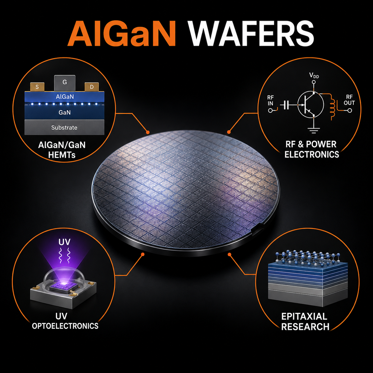
One of the most important applications of AlGaN is its use with Gallium Nitride (GaN). AlGaN/GaN heterostructures can support a two-dimensional electron gas (2DEG), making them valuable for research into HEMTs, RF devices, and high-power electronics.
AlGaN for Ultraviolet Research
Increasing the aluminum content of AlGaN increases its bandgap, allowing researchers to engineer materials for ultraviolet and deep-ultraviolet optoelectronics. Research applications include UV LEDs, photodetectors, sensors, and other short-wavelength devices.
AlGaN Epitaxy and Device Development
Researchers study AlGaN layers grown through techniques such as MOCVD and MBE to develop heterostructures and investigate material quality, interfaces, electrical behavior, and optical properties. Substrate selection and epitaxial structure are important considerations for advanced III-nitride research.
Selecting AlGaN Materials
Important parameters can include Aluminum composition, layer thickness, doping, substrate material, crystal orientation, and epitaxial structure. The appropriate configuration depends on whether the research involves HEMTs, UV optoelectronics, RF electronics, or material characterization.
Get Your AlGaN Wafer Quote FAST! Or Buy Online and Start Researching Today!
AlGaN Properties and Research Applications
Aluminum Gallium Nitride (AlGaN) is a wide-bandgap III-nitride semiconductor alloy used in advanced electronic and optoelectronic research. Its bandgap can be engineered by adjusting the aluminum-to-gallium composition, making AlGaN useful for applications ranging from high-frequency transistors to ultraviolet devices.
AlGaN for HEMT Research
AlGaN is widely studied in High-Electron-Mobility Transistors (HEMTs). AlGaN/GaN heterostructures can form a high-density two-dimensional electron gas (2DEG), supporting research into devices designed for high-frequency and high-power operation.
RF and Power Electronics
The wide-bandgap characteristics of AlGaN make it important for research into RF, microwave, and power semiconductor devices. AlGaN/GaN structures are investigated for technologies that require high electric-field capability, fast switching, and high-frequency performance.
Common AlGaN Research Applications
- HEMTs and transistor research
- RF and microwave electronics
- Power semiconductor devices
- UV and deep-UV LEDs
- Ultraviolet photodetectors
- AlGaN/GaN heterostructures
- Epitaxial growth and thin-film research
- III-nitride material characterization
AlGaN for UV Optoelectronics
AlGaN is particularly valuable for ultraviolet optoelectronics because its bandgap can be tuned through alloy composition. Higher aluminum concentrations enable research at shorter wavelengths, including UV and deep-ultraviolet LEDs, detectors, and sensors.
AlGaN Epitaxial Structures
AlGaN layers and heterostructures can be investigated using epitaxial growth methods such as Metal-Organic Chemical Vapor Deposition (MOCVD) and Molecular Beam Epitaxy (MBE). Researchers study layer composition, thickness, doping, interfaces, strain, and crystal quality to optimize device structures.
Choosing AlGaN Material for Your Research
Important considerations include aluminum composition, layer thickness, doping, substrate type, epitaxial structure, and surface quality. The ideal specifications depend on whether the material will be used for HEMTs, RF electronics, power devices, UV optoelectronics, or fundamental materials research.
UniversityWafer can help researchers source AlGaN and related III-V semiconductor materials for university, laboratory, and advanced semiconductor R&D applications.