
4H-SiC Wafers for Advanced Research
UniversityWafer provides 4H silicon carbide (4H-SiC) wafers for researchers developing next-generation power electronics and wide-bandgap semiconductor technologies. SiC substrates are particularly valuable for experiments requiring high breakdown strength, thermal stability, and reliable operation under demanding electrical conditions.
Researchers can use 4H-SiC substrates for material characterization, device fabrication, epitaxial studies, surface processing, and proof-of-concept experiments involving high-voltage semiconductor devices.
4H-SiC Wafer Specifications to Consider
Selecting the correct SiC substrate can significantly affect experimental results. Important parameters to consider when requesting wafers include:
- Polytype: 4H-SiC
- Conductivity: semi-insulating or conductive
- Doping: n-type or other available configurations
- Orientation: on-axis or specified off-axis orientation
- Surface: Si-face or C-face depending on the experiment
- Finish: polished or double-side polished when available
- Thickness: selected according to process requirements
- Diameter: dependent on research and fabrication equipment
Si-Face vs. C-Face 4H-SiC
The two polar surfaces of silicon carbide can behave differently during oxidation, epitaxial growth, surface preparation, and thin-film deposition. Researchers should therefore specify whether their experiment requires the silicon-terminated (Si-face) or carbon-terminated (C-face) surface.
Surface selection can be especially important for experiments involving epitaxy, MOS structures, dielectric interfaces, and surface chemistry.
Research-Grade SiC for Universities and Laboratories
Not every experiment requires production quantities of semiconductor substrates. Small-quantity SiC wafers allow university laboratories, startups, and R&D teams to evaluate processes and device concepts before moving to larger-scale fabrication.
Applications can include high-voltage device testing, MOS interface studies, oxidation experiments, thin-film deposition, materials characterization, and development of new SiC processing techniques.
High-Voltage SiC Research
The electrical and thermal properties of 4H-SiC make it an important material for research into technologies used in electric vehicles, renewable-energy systems, power converters, industrial electronics, aerospace systems, and electrical-grid infrastructure.
Researchers can investigate device structures designed to achieve higher blocking voltages, reduced power losses, improved thermal performance, and efficient high-frequency switching.
Need a Specific 4H-SiC Wafer?
If your research requires a particular diameter, orientation, thickness, doping level, resistivity, surface finish, or epitaxial configuration, send us your specifications. UniversityWafer can help identify an appropriate 4H-SiC substrate for your experiment.
Get Your 4H-SiC Wafer Quote FAST! Or Buy Online and Start Researching Today!
Why Use 4H-SiC Wafers for High-Voltage Research?
4H silicon carbide (4H-SiC) is one of the most important semiconductor materials for high-power and high-voltage research. Its wide bandgap, high critical electric field, excellent thermal conductivity, and ability to operate at elevated temperatures make it especially valuable for power electronics where conventional silicon can reach its performance limits.
Researchers use 4H-SiC wafers to develop devices capable of handling higher voltages, higher temperatures, and demanding switching conditions while investigating ways to improve power density and device efficiency.
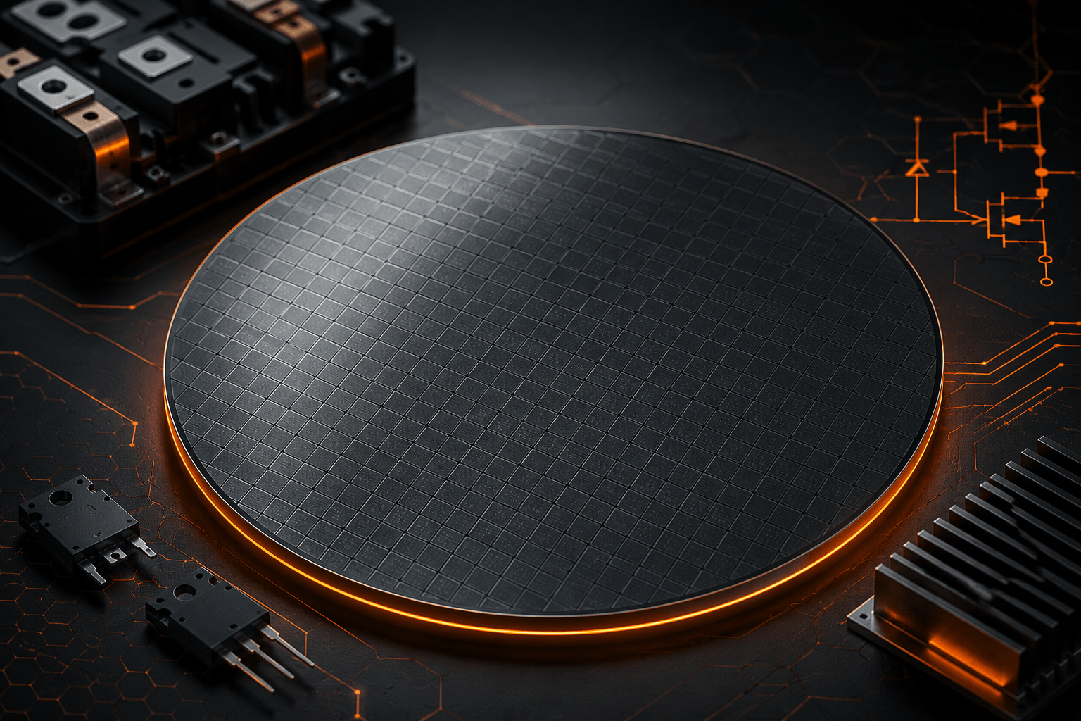
4H-SiC for High-Voltage Power Devices
The high breakdown electric field of 4H-SiC enables researchers to investigate thinner drift regions and high-voltage device architectures. This makes SiC an important substrate platform for the development and characterization of advanced power semiconductor devices.
Common research applications include:
- SiC MOSFETs for high-voltage power switching
- Schottky barrier diodes (SBDs)
- PiN diodes for high-voltage device research
- Junction barrier Schottky (JBS) diodes
- Power device breakdown and reliability studies
- High-temperature semiconductor electronics
- SiC epitaxial layer development and characterization
Why 4H-SiC Instead of Silicon?
Silicon remains an essential substrate for semiconductor research, but 4H-SiC provides material properties that are particularly attractive when researchers investigate high-voltage, high-temperature, and high-power applications.
| Property | 4H-SiC | Silicon |
|---|---|---|
| Bandgap | ~3.26 eV | ~1.12 eV |
| Critical Electric Field | ~2.5–3 MV/cm | ~0.3 MV/cm |
| Thermal Conductivity | High | Moderate |
| High-Temperature Operation | Excellent | More Limited |
| Typical Research Focus | High-voltage and high-power devices | Conventional semiconductor devices |
4H-SiC Wafer Research Applications
University and industrial laboratories use 4H-SiC substrates across a wide range of experimental power semiconductor projects. Applications extend beyond individual device fabrication to material characterization, surface processing, thin-film deposition, and epitaxial research.
- Wide-bandgap semiconductor research
- High-voltage device fabrication
- SiC MOSFET development and testing
- Power conversion research
- Electric vehicle power electronics
- Renewable energy and grid power systems
- Aerospace and high-temperature electronics
- Epitaxial growth and thin-film studies
- Surface processing and interface research
Selecting a 4H-SiC Research Wafer
The appropriate wafer specification depends on the experiment and fabrication process. Researchers may need to consider wafer diameter, conductivity type, doping, crystal orientation, thickness, surface finish, resistivity, and epitaxial layer requirements.
Both production-grade and research-oriented substrates can be useful depending on whether the project requires device fabrication, process development, material characterization, or preliminary experiments.
4H-SiC Substrates for Research and Development
UniversityWafer supplies semiconductor substrates for universities, government laboratories, startups, and industrial R&D programs. Researchers can request specifications suited to experiments involving silicon carbide power devices, high-voltage electronics, epitaxy, surface characterization, and wide-bandgap semiconductor technology.
Small quantities can be especially useful for proof-of-concept experiments and early-stage research where purchasing full production volumes is unnecessary.