Need Silicon Epitaxy Wafers?
Get Your Silicon Epitaxy Wafer Quote FAST! Or Buy Online for premium epitaxial silicon wafers used in integrated circuits, power electronics, MEMS, and semiconductor research.
Silicon epitaxy wafers feature a precisely grown single-crystal silicon layer deposited on a silicon substrate to achieve superior electrical performance, controlled doping, and exceptional crystal quality. Widely used in integrated circuits, power semiconductors, MEMS, sensors, analog devices, and RF technologies, epitaxial silicon wafers provide the uniformity and reliability required for advanced semiconductor manufacturing. UniversityWafer supplies custom silicon epitaxy wafers with a wide range of layer thicknesses, resistivities, crystal orientations, and doping options for research, prototyping, and commercial production.

Silicon epitaxy is the process of growing a high-purity single-crystal silicon layer on a monocrystalline silicon substrate. This epitaxial layer provides precise control over thickness, resistivity, and dopant concentration while maintaining the crystal orientation of the underlying wafer. The result is a substrate ideally suited for manufacturing high-performance integrated circuits, power devices, MEMS, RF components, and advanced sensors.
UniversityWafer supplies custom epitaxial wafers with a wide range of epitaxial layer thicknesses, crystal orientations, resistivities, and doping profiles. We also offer silicon wafers, research substrates, wafer processing services, and III-V semiconductor wafers to support advanced semiconductor fabrication.
UniversityWafer can source silicon epitaxy wafers with custom epitaxial layer thicknesses, doping concentrations, resistivity ranges, wafer diameters, polishing options, and crystal orientations. Whether you require N-type or P-type epitaxial layers for research or production, our engineering team can help identify the appropriate wafer for your application.
Get Your Silicon Epitaxy Wafer Quote FAST! Or Buy Online for premium epitaxial silicon wafers used in integrated circuits, power electronics, MEMS, and semiconductor research.
Silicon epitaxy is the process of growing a thin, single-crystal layer of silicon on top of a monocrystalline silicon wafer. Because the deposited layer follows the crystal structure of the underlying substrate, the resulting epitaxial wafer exhibits excellent crystal quality, precisely controlled dopant concentrations, and uniform electrical characteristics. Silicon epitaxy is a critical technology used to manufacture high-performance integrated circuits, power devices, MEMS, sensors, and RF components.
Most silicon epitaxial layers are deposited using Chemical Vapor Deposition (CVD), allowing manufacturers to precisely control layer thickness, resistivity, and dopant profiles for advanced semiconductor device fabrication.
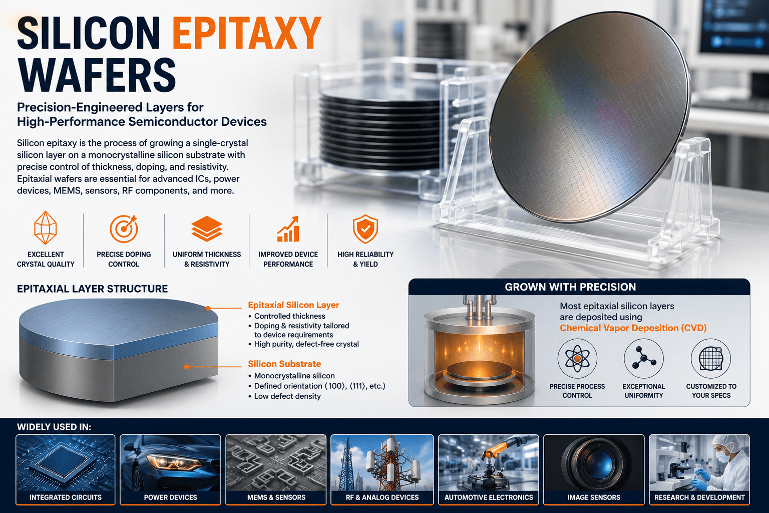
Silicon epitaxial wafers are widely used throughout the semiconductor industry where precise electrical control and high device reliability are required. Typical applications include:
UniversityWafer supplies custom silicon epitaxy wafers with multiple epitaxial layer thicknesses, wafer diameters, crystal orientations, doping profiles, resistivities, and polishing options. Both N-type and P-type epitaxial layers are available for research, prototype development, and commercial semiconductor manufacturing.
We also supply epitaxial wafers, silicon wafers, research substrates, and wafer processing services to support semiconductor fabrication and advanced materials research.
Modern semiconductor devices demand exceptional electrical uniformity, low defect densities, and tightly controlled material properties. Silicon epitaxy enables engineers to optimize device performance by tailoring the electrical characteristics of the active silicon layer without altering the underlying substrate. This capability makes epitaxial silicon wafers indispensable for today's integrated circuits, power electronics, automotive systems, telecommunications, and next-generation semiconductor technologies.